MIC5265
150mA µCap LDO Regulator
Micrel Inc. ∑ 2180 Fortune Drive ∑ San Jose, CA 95131 ∑ USA ∑ tel +1 (408) 944-0800 ∑ fax + 1 (408) 474-1000 ∑ http://www.micrel.com
April 2005
M9999-041505
(408) 955-1690
General Description
The MIC5265 is a 150mA LDO in lead-free Thin SOT-23-5
packaging ideal for applications where cost is the priority.
The MIC5265 is ideal for any application in portable
electronics, including both RF and Digital applications.
With low output noise and high PSRR, the MIC5265 is
ideal for noise sensitive applications such as RF. While
the fast transient response and active shutdown circuitry
makes it well-suited for powering digital circuitry.
The MIC5265 has a 2.7V to 5.5V input operating voltage
range, making it ideal for operation from a single cell
lithium ion battery or fixed 3.3V and 5V systems. The
MIC5265 come with an enable pin and can be put into a
zero off-mode current state.
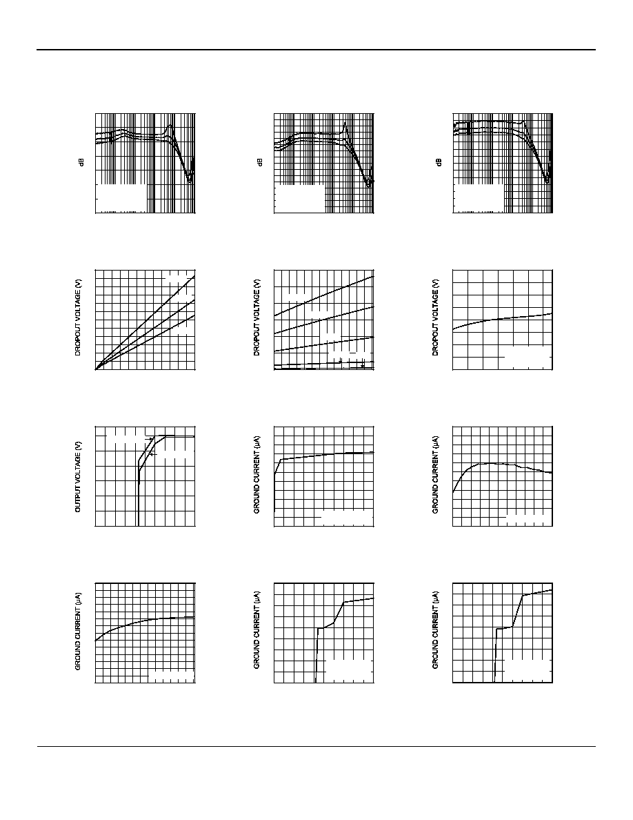
The MIC5265 offers low dropout voltage (210mV at
150mA), low output noise (57µVrms), high PSRR and
integrates an active shutdown circuit on the output of each
regulator to discharge the output voltage when disabled.
Data sheets and supporting documentation can be found
on Micrel's web site at: www.micrel.com
Features
∑
2.7V to 5.5V supply voltage.
∑
Low 75µA quiescent current per LDO.
∑
Thin SOT-23-5 package.
∑
Low Noise ≠ 57µVrms.
∑
High PSRR ≠ 60dB at 1kHz.
∑
Low dropout voltage ≠ 210mV at 150mA.
∑
Stable with ceramic output capacitors.
∑
Fast transient response.
∑
Active shutdown.
Applications
∑
Cellular
Telephones
∑
PDAs
∑
GPS
Receivers
____________________________________________________________________________________________________________
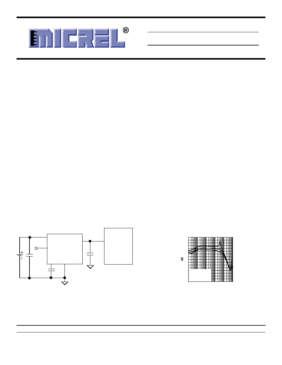
Typical Application
MIC5265-xxYD5
VIN
VOUT
BYP
GND
EN
Rx/Synth
RF Receiver
0.01µF
1µF
1µF
RF Power Supply
0
-10
-20
-40
-50
-60
-70
0.01 0.1
1 10 100 1000
FREQUENCY (kHz)
Power Supply
Rejection Ratio
-30
-80
V
IN
= V
OUT
+ 1V
V
OUT
= 3.1V
BYP = 0.1µF
C
OUT
= 1µF
Micrel, Inc.
MIC5265
April 2005
4
M9999-041505
(408) 955-1690
Absolute Maximum Ratings
(1)
Supply Input Voltage (V
IN
).................................... 0V to +7V
Enable Input Voltage (V
EN1
) ................................. 0V to +7V
Power Dissipation (P
D
) .......................... Internally Limited
(3)
Junction Temperature (T
J
) ...........................-40∞C to 125∞C
Lead Temperature (soldering, #sec.)...........-55∞C to 150∞C
Storage Temperature (T
s
) .......................................... 260∞C
EDS Rating
(4)
................................................................. 2kV
Operating Ratings
(2)
Supply Input Voltage (V
IN
)............................ +2.7V to +5.5V
Enable Input Voltage (V
EN
)................................... 0V to +V
IN
Junction Temperature (T
A
) ........................ ≠40∞C to +125∞C
Junction Thermal Resistance
Thin SOT-23-5 (
JA
).........................................235∞C/W
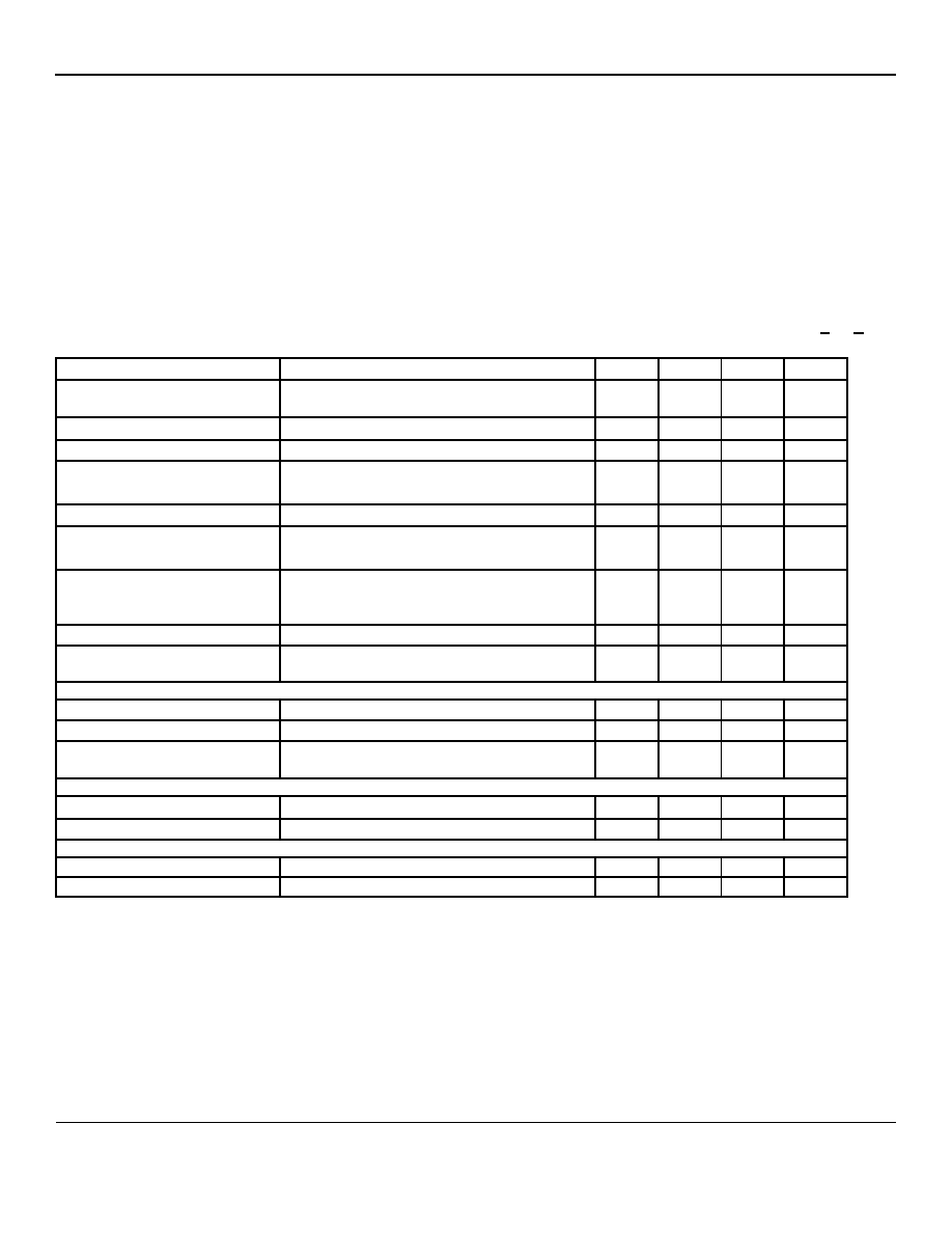
Electrical Characteristics
(5)
V
EN
= V
IN
= V
OUT
+ 1V; I
L
=100µA; C
L
= 1.0µF; C
BYP
= 0.01µF per output; T
A
= 25∞C, bold values indicate ≠40∞C< T
A
<
+85∞C; unless noted.
Parameter
Condition
Min
Typ
Max
Units
Output Voltage Accuracy
I
OUT
= 100
µ
A
-2
-3
2
3
%
%
Line Regulation
V
IN
= V
OUT
+1V to 5.5V
0.05
0.2
%
Load Regulation
I
OUT
= 0.1mA to 150mA
2
3
%
Dropout Voltage
I
OUT
= 50mA
I
OUT
= 150mA
75
210
500
mV
mV
Quiescent Current
V
EN
< 0.2V
0.2
2
µ
A
Ground Pin Current
I
OUT
= 0mA
I
OUT
= 150mA
75
80
120
150
µ
A
µ
A
PSRR (Ripple Rejection)
f = 100Hz, C
BYP
= 0.1
µ
F, I
LOAD
≠ 50mA
f = 1kHz, C
BYP
= 0.1
µ
F, I
LOAD
≠ 50mA
f = 10kHz, C
BYP
= 0.1
µ
F, I
LOAD
≠ 50mA
62
64
64
dB
dB
dB
Current Limit
V
OUT
= 0V
225
mA
Output Noise
C
OUT
= 1.0
µ
F, C
BYP
= 0.1
µ
F, f = 10Hz to
100kHz
57
µ
V
(rms)
Enable Input (EN1 and EN2)
Enable Input Logic Low
V
IN
= 2.7V to 5.5V, regulator shutdown
0.2
V
Enable Input Logic High
V
IN
= 2.7V to 5.5V, regulator enabled
1.6
V
Enable Input Current
V
IL
< 0.4V, regulator shutdown
V
IH
> 1.6V, regulator enabled
0.01
0.01
µ
A
µ
A
Thermal Shutdown
Thermal Shutdown Temperature
150
∞C
Hysteresis
10
∞C
Turn-on/Turn-off Characteristics
Turn-on Time
40
150
µ
s
Discharge Resistance
500
Notes:
1.
Exceeding the absolute maximum rating may damage the device.
2.
The device is not guaranteed to function outside its operating rating.
3.
The maximum allowable power dissipation of any T
A
(ambient temperature) is P
D(max)
= (T
J(max)
≠T
A
)/
JA
. Exceeding the maximum allowable
power dissipation will result in excessive die temperature, and the regulator will go into thermal shutdown. The
JA
of the MIC5265x.xYD5 (all
versions) is 235
∞
C/W on a PC board (see "Thermal Considerations" section for further details).
4.
Devices are ESD sensitive. Handling precautions recommended. Human body model, 1.5k in series with 100pF.
5.
Specification for packaged product only.