
March 1999
283
MIC5270
MIC5270
Micrel
MIC5270
IttyBittyTM Negative Low-Dropout Regulator
Preliminary Information
General Description
The MIC5270 is a
µ
Cap 100mA negative regulator in a SOT-
23-5 package. With better than 2% initial accuracy, this
regulator provides a very accurate supply voltage for applica-
tions that require a negative rail. The MIC5270 sinks 100mA
of output current at very low dropout voltage (600mV maxi-
mum at 100mA of output current).
The
µ
Cap regulator design is optimized to work with low-
value, low-cost ceramic capacitors. The output typically re-
quires only a 1
µ
F capacitance for stability.
Designed for applications where small packaging and effi-
ciency are critical, the MIC5270 combines LDO design exper-
tise with IttyBitty
TM
packaging to improve performance and
reduce power dissipation. Ground current is optimized to help
improve battery life in portable applications.
The MIC5270 is available in the SOT-23-5 package for space
saving applications and it is available with fixed ≠3.0V, ≠4.1V,
and ≠5.0V outputs.
Typical Application
MIC5270-5.0
GND
≠OUT
≠IN
1µF
10µF
≠5.0V
≠6.0V
V
IN
2
5
4
V
OUT
Features
∑ IttyBitty
TM
SOT-23-5 packaging
∑ Low dropout voltage
∑ Low ground current
∑ Tight initial accuracy
∑ Tight load and line regulation
∑ Thermal shutdown
∑ Current limiting
∑ Stable with low-ESR ceramic capacitors
Applications
∑ GaAsFET bias
∑ Portable cameras and video recorders
∑ PDAs
∑ Battery-powered equipment
IttyBitty is a trademark of Micrel, Inc.
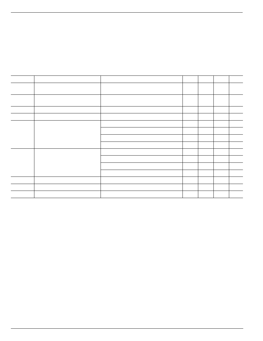
Ordering Information
Part Number
Voltage
Temperature Range
Package
MIC5270-3.0BM5
≠3.0V
≠40
∞
C to +85
∞
C
SOT-23-5
MIC5270-4.1BM5
≠4.1V
≠40
∞
C to +85
∞
C
SOT-23-5
MIC5270-5.0BM5
≠5.0V
≠40
∞
C to +85
∞
C
SOT-23-5
Pin Configuration
NC
≠IN
≠OUT
NC
LLxx
1
3
4
5
2
GND
MIC5270-x.xBM5
Pin Description
Pin Number
Pin Name
Pin Function
1
NC
Not internally connected.
2
GND
Ground
3
NC
Not internally connected.
4
≠OUT
Negative Regulator Output
5
≠IN
Negative Supply Input
MIC5270
Micrel
MIC5270
284
March 1999
Absolute Maximum Ratings
(Note 1)
Input Voltage (V
≠IN
) ....................................... ≠20V to +20V
Power Dissipation (P
D
) ............................ Internally Limited
Junction Temperature (T
J
) ....................... ≠40
∞
C to +125
∞
C
Lead Temperature (soldering, 5 sec.) ....................... 260
∞
C
Storage Temperature (T
S
) ....................... ≠65
∞
C to +150
∞
C
ESD Rating, Note 3
Operating Ratings
(Note 2)
Input Voltage (V
IN
) .......................................... ≠16V to ≠2V
Junction Temperature (T
J
) ....................... ≠40
∞
C to +125
∞
C
Thermal Resistance (
JA
) ......................................... Note 4
Electrical Characteristics
V
IN
= V
OUT
≠ 1.0V; C
OUT
= 4.7
µ
F, I
OUT
= 100
µ
A; T
J
= 25
∞
C, bold values indicate ≠40
∞
C
T
J
+125
∞
C; unless noted.
Symbol
Parameter
Condition
Min
Typ
Max
Units
V
OUT
Output Voltage Accuracy
Variation from nominal V
OUT
≠2
2
%
≠3
3
%
V
OUT
/
T
Output Voltage Temperature
Note 5
100
ppm/
∞
C
Coefficient
V
OUT
/V
OUT
Line Regulation
V
IN
= V
OUT
≠ 1V to ≠16V
0.055
0.15
%/V
V
OUT
/V
OUT
Load Regulation
I
OUT
= 100
µ
A to 100mA, Note 6
2.0
%
V
IN
≠ V
OUT
Dropout Voltage, Note 7
I
OUT
= 100
µ
A
35
mV
I
OUT
= 10mA
250
mV
I
OUT
= 50mA
360
450
mV
I
OUT
= 100mA
480
600
mV
I
GND
Ground Current, Note 8
I
OUT
= 100
µ
A
70
µ
A
I
OUT
= 10mA
250
µ
A
I
OUT
= 50mA
0.7
mA
I
OUT
= 100mA
2.1
3.0
mA
PSRR
Ripple Rejection
f = 120Hz
50
dB
I
LIMIT
Current Limit
V
OUT
= 0V
160
300
mA
V
OUT
/
P
D
Thermal Regulation
Note 9
0.05
%/W
Note 1.
Exceeding the absolute maximum rating may damage the device.
Note 2.
The device is not guaranteed to function outside its operating rating.
Note 3.
Devices are ESD sensitive. Handling precautions recommended.
Note 4.
The maximum allowable power dissipation is a function of the maximum junction temperature, T
J(max)
, the junction-to-ambient thermal
resistance,
JA
, and the ambient temperature, T
A
. The maximum allowable power dissipation at any ambient temperature is calculated using:
P
D(max)
= (T
J(max)
≠ T
A
)
˜
JA
, where
JA
is 235
∞
C/W. Exceeding the maximum allowable power dissipation will result in excessive die
temperature, and the regulator will go into thermal shutdown. See the "Thermal Considerations" section for details.
Note 5.
Output voltage temperature coefficient is defined as the worst case voltage change divided by the total temperature range.
Note 6.
Regulation is measured at constant junction temperature using low duty cycle pulse testing. Parts are tested for load regulation in the load
range from 100
µ
A to 100mA. Changes in output voltage due to heating effects are covered by the thermal regulation specification.
Note 7.
Dropout voltage is defined as the input to output differential at which the output voltage drops 2% below its nominal value measured at 1V
differential.
Note 8.
Ground pin current is the regulator quiescent current plus pass transistor base current. The total current drawn from the supply is the sum of
the load current plus the ground pin current.
Note 9.
Thermal regulation is defined as the change in output voltage at a time "t" after a change in power dissipation is applied, excluding load or line
regulation effects. Specifications are for a 100mA load pulse at V
IN
= ≠16V for t = 10ms.
March 1999
285
MIC5270
MIC5270
Micrel
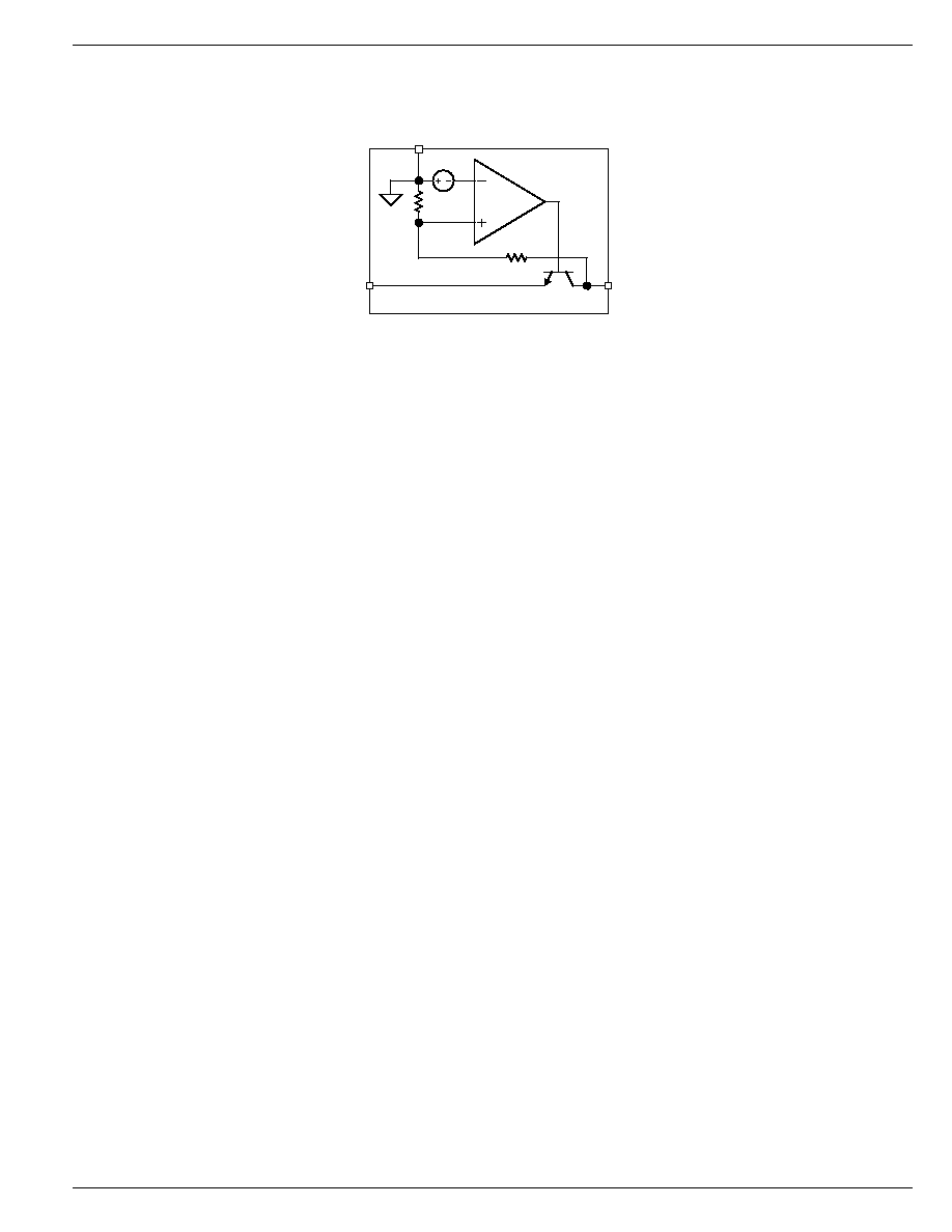
Functional Diagram
V
IN
V
OUT
GND
MIC5270-x.x

MIC5270
Micrel
MIC5270
286
March 1999
Applications Information
The MIC5270 is a general-purpose negative regulator that
can be used in any system that requires a clean negative
voltage from a negative output. This includes post regulating
of dc-dc converters (transformer based or charge pump
based voltage converters). These negative voltages typically
require a negative low-dropout voltage regulator to provide a
clean output from typically noisy lines.
Input Capacitor
A 1
µ
F input capacitor should be placed from IN to GND if
there is more than 2 inches of wire or trace between the input
and the ac filter capacitor, or if a battery is used as the input.
Output Capacitor
The MIC5270 requires an output capacitor for stable opera-
tion. A minimum of 1
µ
F of output capacitance is required. The
output capacitor can be increased without limitation to im-
prove transient response. The output does not require ESR
to maintain stability, therefore a ceramic capacitor can be
used. High-ESR capacitors may cause instability. Capacitors
with an ESR of 3
or greater at 100kHz may cause a high
frequency oscillation.
Low-ESR tantalums are recommended due to the tight ca-
pacitance tolerance over temperature.
Ceramic chip capacitors have a much greater dependence
on temperature, depending upon the dielectric. The X7R is
recommended for ceramic capacitors because the dielectric
will change capacitance value by approximately 15% over
temperature. The Z5U dielectric can change capacitance
value by as much 50% over temperature, and the Y5V
dielectric can change capacitance value by as much as 60%
over temperature. To use a ceramic chip capacitor with the
Y5V dielectric, the value must be much higher than a tanta-
lum to ensure the same minimum capacitor value over
temperature.
No-Load Stability
The MIC5270 does not require a load for stability.
Thermal Considerations
Absolute values will be used for thermal calculations to clarify
what is meant by power dissipation and voltage drops across
the part.
Proper thermal design for the MIC5270-5.0BM5 can be
accomplished with some basic design criteria and some
simple equations. The following information must be known
to implement your regulator design:
V
IN
= input voltage
V
OUT
= output voltage
I
OUT
= output current
T
A
= ambient operating temperature
I
GND
= ground current
Maximum power dissipation can be determined by knowing
the ambient temperature, T
A
, the maximum junction tem-
perature, 125
∞
C, and the thermal resistance, junction to
ambient. The thermal resistance for this part, assuming a
minimum footprint board layout, is 235
∞
C/W. The maximum
power dissipation at an ambient temperature of 25
∞
C can be
determined with the following equation:
P
T
T
D(max)
J(max)
A
JA
=
-
P
125 C
25 C
235 C/W
D(max)
=
∞ -
∞
∞
P
425mW
D(max)
=
The actual power dissipation of the regulator circuit can be
determined using one simple equation.
P
V
V
I
V
I
D
IN
OUT
OUT
IN
GND
=
-
(
)
+
Substituting P
D(max)
, determined above, for P
D
and solving
for the operating conditions that are critical to the application
will give the maximum operating conditions for the regulator
circuit. The maximum power dissipation number cannot be
exceeded for proper operation of the device. The maximum
input voltage can be determined using the output voltage of
5.0V and an output current of 100mA. Ground current, of 1mA
for 100mA of output current, can be taken from the Electrical
Characteristics section of the data sheet.
425mW
V
5.0V 100mA
V
1mA
IN
IN
=
-
(
)
+
425mW
100mA V
1mA V
500mW
IN
IN
=
+
(
)
-
925mW
101mA V
IN
=
V
9.16Vmax
IN
=
Therefore, a ≠5.0V application at 100mA of output current
can accept a maximum input voltage of ≠9.16V in a SOT-23-5
package. For a full discussion of heat sinking and thermal
effects on voltage regulators, refer to Regulator Thermals
section of Micrel's Designing with Low-Dropout Voltage Regu-
lators handbook.