June 2003
1
MIC5271
MIC5271
Micrel
MIC5271
µ
Cap Negative Low-Dropout Regulator
General Description
The MIC5271 is a
µ
Cap 100mA negative regulator in a SOT-
23-5 package. With better than 2% initial accuracy, this
regulator provides a very accurate supply voltage for applica-
tions that require a negative rail. The MIC5271 sinks 100mA
of output current at very low dropout voltage (600mV maxi-
mum at 100mA of output current).
The
µ
Cap regulator design is optimized to work with low-
value, low-cost ceramic capacitors. The output typically re-
quires only a 1
µ
F capacitance for stability.
Designed for applications where small packaging and effi-
ciency are critical, the MIC5271 combines LDO design exper-
tise with IttyBitty
Æ
packaging to improve performance and
reduce power dissipation. Ground current is optimized to help
improve battery life in portable applications. The MIC5271
also includes a TTL-compatible enable pin, allowing the user
to put the part into a zero-current off-mode.
The MIC5271 is available in the SOT-23-5 package for space
saving applications and it is available with an adjustable
output.
Data sheets and support documentation can be found on
Micrel's web site at www.micrel.com.
Typical Application
Features
∑ Stable with ceramic or tantalum capacitor
∑ Low dropout voltage: 500mV @ 100mA
∑ Low ground current: 35
µ
A @ load = 100
µ
A
∑ Tight initial accuracy:
±
2%
∑ Tight load and line regulation
∑ Thermal shutdown
∑ Current limiting
∑ IttyBitty
Æ
SOT-23-5 packaging
∑ Zero-current off-mode
Applications
∑ GaAsFET bias
∑ Portable cameras and video recorders
∑ PDAs
∑ Battery-powered equipment
IttyBitty is a registered trademark of Micrel, Inc.
Micrel, Inc. ∑ 1849 Fortune Drive ∑ San Jose, CA 95131 ∑ USA ∑ tel + 1 (408) 944-0800 ∑ fax + 1 (408) 944-0970 ∑ http://www.micrel.com
Ordering Information
Part Number
Marking
Voltage*
Junction Temp. Range
Package
MIC5271BM5
L9AA
Adj.
≠40
∞
C to +125
∞
C
SOT-23-5
* For other voltage options, please contact Micrel Marketing.
MIC5271BM5
GND
EN
≠OUT
≠IN
1
µ
F
10
µ
F
≠5.0V
≠6.0V
V
IN
2
5
1
4
3
V
R1
R2
OUT
ADJ
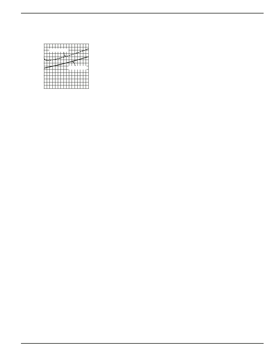
Regulator With Fixed Output
-5
-4
-3
-2
-1
0
1
2
3
4
5
-3
-5
-7
-9
-11 -13 -15
ENABLE VOLTAGE (V)
SUPPLY VOLTAGE (V)
Enable Input
Regulator On
Regulator On
Regulator Off

June 2003
3
MIC5271
MIC5271
Micrel
Absolute Maximum Ratings
(Note 1)
Input Voltage (V
≠IN
) ...................................... ≠20V to +0.3V
Enable Voltage (V
EN
) .................................... ≠20V to +20V
Power Dissipation (P
D
) ............................ Internally Limited
Junction Temperature (T
J
) ....................... ≠40
∞
C to +125
∞
C
Lead Temperature (soldering, 5 sec.) ....................... 260
∞
C
Storage Temperature (T
S
) ....................... ≠65
∞
C to +150
∞
C
ESD Rating, Note 3
Operating Ratings
(Note 2)
Input Voltage (V
IN
) ....................................... ≠16V to ≠3.3V
Enable Voltage (V
EN
) .................................... ≠16V to +16V
Junction Temperature (T
J
) ....................... ≠40
∞
C to +125
∞
C
Thermal Resistance (
JA
) Note 4 ......................... 235
∞
C/W
Electrical Characteristics
(Note 5)
V
IN
= V
OUT
≠ 1.0V; C
OUT
= 4.7
µ
F, I
OUT
= 100
µ
A; T
J
= 25
∞
C, bold values indicate ≠40
∞
C
T
J
+125
∞
C; unless noted.
Symbol
Parameter
Condition
Min
Typ
Max
Units
V
OUT
Output Voltage Accuracy
Variation from nominal V
OUT
≠2
2
%
≠3
3
%
V
OUT
/
T
Output Voltage Temperature
Note 6
100
ppm/
∞
C
Coefficient
V
OUT
/V
OUT
Line Regulation
V
IN
= V
OUT
≠ 1V to ≠16V
0.04
0.15
%/V
0.2
V
OUT
/V
OUT
Load Regulation
I
OUT
= 100
µ
A to 100mA, Note 7
0.4
1.8
%
2.0
%
V
IN
≠ V
OUT
Dropout Voltage, Note 8
I
OUT
= 100
µ
A
55
mV
I
OUT
= 50mA
360
500
mV
I
OUT
= 100mA
500
700
mV
900
I
GND
Ground Current, Note 9
I
OUT
= 100
µ
A
25
100
µ
A
I
OUT
= 50mA
0.9
mA
I
OUT
= 100mA
2.0
3.0
mA
PSRR
Ripple Rejection
f = 120Hz
50
dB
I
LIMIT
Current Limit
V
OUT
= 0V
235
350
mA
Enable Input
T
ON
Turn-on Time
Time to V
OUT
= 90% nom.
60
µ
s
V
EN
Input Low voltage
Regulator OFF
±
0.6
V
Input High Voltage
Regulator ON
±
2.0
V
I
EN
Enable Input Current
V
EN
=
±
0.6V and ≠2.0V
0.1
µ
A
V
EN
= +2.0V
5.6
10.0
Note 1.
Exceeding the absolute maximum rating may damage the device.
Note 2.
The device is not guaranteed to function outside its operating rating.
Note 3.
Devices are ESD sensitive. Handling precautions recommended.
Note 4.
The maximum allowable power dissipation is a function of the maximum junction temperature, T
J(max)
, the junction-to-ambient thermal
resistance,
JA
, and the ambient temperature, T
A
. The maximum allowable power dissipation at any ambient temperature is calculated using:
P
D(max)
= (T
J(max)
≠ T
A
) /
JA
, where
JA
is 235
∞
C/W. Exceeding the maximum allowable power dissipation will result in excessive die
temperature, and the regulator will go into thermal shutdown. See the
"Thermal Considerations"
section for details.
Note 5.
Specification for packaged product only.
Note 6.
Output voltage temperature coefficient is defined as the worst case voltage change divided by the total temperature range.
Note 7.
Regulation is measured at constant junction temperature using low duty cycle pulse testing. Parts are tested for load regulation in the load
range from 100
µ
A to 100mA. Changes in output voltage due to heating effects are covered by the thermal regulation specification.
Note 8.
Dropout voltage is defined as the input to output differential at which the output voltage drops 2% below its nominal value measured at 1V
differential.
Note 9.
Ground pin current is the regulator quiescent current plus pass transistor base current. The total current drawn from the supply is the sum of
the load current plus the ground pin current.