
MIC5307
300mA Micropower µCap
Baseband LDO
Micrel Inc. ∑ 2180 Fortune Drive ∑ San Jose, CA 95131 ∑ USA ∑ tel +1 (408) 944-0800 ∑ fax + 1 (408) 474-1000 ∑ http://www.micrel.com
October 2006
1
M9999-102706-A
General Description
The MIC5307 is a micropower, µCap low dropout regulator
designed for optimal performance where smaller packages
are required. It is capable of sourcing 300mA of output
current while only drawing 20µA of operating current. This
high performance LDO offers fast transient response and
good PSRR while consuming a minimum of current.
Ideal for battery operated applications; the MIC5307 offers
1% initial accuracy, extremely low dropout voltage and is
equipped with a TTL logic compatible enable pin. The
MIC5307 can be put into a zero-off-mode current state,
drawing no current when disabled.
The MIC5307 is a µCap design, operating with very small
ceramic output capacitors for stability, reducing required
board space and component cost.
The MIC5307 is available in fixed output voltages in the
Thin SOT23-5 package.
Data sheets and support documentation can be found on
Micrel's web site at www.micrel.com.
Features
∑
Input voltage range: 2.4V to 5.5V
∑
Ultra-low IQ: Only 20µA operating current
∑
Stable with ceramic output capacitor
∑
Low dropout voltage of 120mV @ 300mA
∑
High output accuracy
≠ ±1.0% initial accuracy
≠ ±2.0% over temperature
∑
Thermal Shutdown Protection
∑
Current Limit Protection
Applications
∑
Digital Logic Power Supply
∑
Stand-by power supply
∑
Cellular phones
∑
PDAs
∑
Portable electronics
∑
Notebook PCs
Typical Application
VOUT
VIN
EN
GND
2.2µF
1µF
MIC5307
0
2
4
6
8
10
12
14
20
22
24
26
20 40 60 80
TEMPERATURE (∞C)
Ground Pin Current
vs. Temperature
V
IN
= V
OUT
+ 1V
V
OUT
= 2.8V
C
OUT
= 2.2µF
100µA
300mA
16
18
Micrel, Inc.
MIC5307
October 2006
4
M9999-102706-A
Absolute Maximum Ratings
(1)
Supply Voltage (V
IN
)............................................... 0V to 6V
Enable Input Voltage (V
EN
)..................................... 0V to 6V
Power Dissipation (P
D
)
(3)
...........................Internally Limited
Junction Temperature (T
J
) ........................≠40∞C to +125∞C
Lead Temperature (soldering, 5sec.)......................... 260∞C
Storage Temperature (T
s
) .........................≠65∞C to +150∞C
ESD Rating
(4)
.................................................................. 2kV
Operating Ratings
(2)
Supply voltage (V
IN
) ....................................... 2.4V to +5.5V
Enable Input Voltage.............................................. 0V to V
IN
Junction Temperature (T
J
) ........................ ≠40∞C to +125∞C
Thermal Resistance
TSOT23-5
(
JA
)................................................235∞C/W
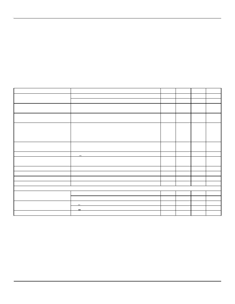
Electrical Characteristics
(5)
V
IN
= V
OUT
+ 1.0V; C
OUT
= 2.2µF; I
OUT
= 100µA; T
J
= 25∞C, bold values indicate ≠40∞C to +125∞C, unless noted.
Parameter Condition
Min
Typ
Max
Units
Variation from nominal V
OUT
≠1
+1
%
Output Voltage Accuracy
Variation from nominal V
OUT
; ≠40∞C to +125∞C
≠2 +2 %
Line Regulation
V
IN
= V
OUT
+1V to 5.5V
0.01
0.3
0.5
%/V
%/V
Load Regulation
I
OUT
= 100µA to 300mA
0.5
1
1.5
%
%
Dropout Voltage
(4)
I
OUT
= 50mA
I
OUT
= 100mA
I
OUT
= 150mA
I
OUT
= 300mA
20
40
60
120
250
mV
mV
mV
mV
Ground Pin Current
I
OUT
= 0mA to 150mA; V
IN
= 5.5V
I
OUT
= 0mA to 300mA; V
IN
= 5.5V
18
20
30
µA
µA
Ground Pin Current in Shutdown
V
EN
< 0.2V; V
IN
= 5.5V
0.01
1
µA
Ripple Rejection
f = 10Hz to 1kHz; C
OUT
= 2.2µF; I
OUT
= 300mA
f = 20kHz; C
OUT
= 2.2µF; I
OUT
= 300mA
62
35
dB
dB
Current Limit
V
OUT
= 0V
350
500
800
mA
Thermal
Shutdown
160 ∞C
Thermal Shutdown Hysteresis
20
∞C
Output Voltage Noise
C
OUT
= 2.2µF; 10Hz to 100kHz
80
µV
RMS
Enable Input
Logic Low
0.2
V
Enable Input Voltage
Logic High
1.0
V
V
IL
< 0.2V
0.01
1
µA
Enable Input Current
V
IH
> 1.0V
0.01
1
µA
Turn-on Time
(6)
C
OUT
= 2.2µF
270
500
µs
Notes:
1. Exceeding the absolute maximum rating may damage the device.
2. The device is not guaranteed to function outside its operating rating.
3. The maximum allowable power dissipation of any T
A
(ambient temperature) is P
D(max)
= T
J(max)
≠ T
A
/
JA
. Exceeding the maximum allowable
power dissipation will result in excessive die temperature, and the regulator will go into thermal shutdown.
4. Devices are ESD sensitive. Handling precautions recommended.
5. Specification for packaged product only.
6. Turn-on time is measured from V
EN
= 1V of the positive edge of the enable signal to 90% of the rising edge of the output voltage of the regulator.


