 | –≠–ª–µ–∫—Ç—Ä–æ–Ω–Ω—ã–π –∫–æ–º–ø–æ–Ω–µ–Ω—Ç: MIC5312 | –°–∫–∞—á–∞—Ç—å:  PDF PDF  ZIP ZIP |

MIC5312
LowQTM Mode Dual 300mA LDO
with Integrated POR
MLF and
Micro
LeadFrame are trademarks of Amkor Technology, Inc.
Micrel Inc. ∑ 2180 Fortune Drive ∑ San Jose, CA 95131 ∑ USA ∑ tel +1 (408) 944-0800 ∑ fax + 1 (408) 474-1000 ∑ http://www.micrel.com
February 2005
M9999-021105
(408) 955-1690
General Description
The MIC5312 is a high performance, dual µCap low
dropout regulator with integrated power-on reset
supervisor, offering ultra-low operating current and a
second, even lower operating current mode, LowQTM
mode, reducing operating current by 75%. Each
regulator can source up to 300mA of output current
maximum.
Ideal for battery operated applications, the MIC5312
offers 1% accuracy, extremely low dropout voltage
(60mV @ 150mA), and low ground current (typically
28µA total). When put into LowQTM mode, the internal
current draw drops down to 7µA total. The MIC5312
also comes equipped with a TTL logic compatible
enable pin that allows the part to be put into a zero-off-
mode current state, drawing no current when disabled.
The Power-on Reset is active low and indicates an
output undervoltage condition on either regulator 1 or 2
when the regulator is enabled.
The MIC5312 is a µCap design, operating with very
small ceramic output capacitors for stability, reducing
required board space and component cost.
The MIC5312 is available in fixed output voltages in the
3mm x 3mm MLF-10 leadless package. Data sheets
and support documentation can be found on Micrel's
web site at www.micrel.com.
Features
∑ Input voltage range: 2.5V to 5.5V
∑ LowQTM Mode
- 7µA total quiescent current
- 10mA output current capable LowQTM mode
- Logic level control with external pin
∑ Stable with ceramic output capacitor
∑ 2 LDO Outputs ≠ 300mA each
∑ Integrated Power-on Reset (POR) with adjustable
delay time
∑ Tiny 3mm x 3mm MLFTM-10 package
∑ Low dropout voltage of 60mV @ 150mA
∑ Ultra-low quiescent current of 28µA total in Full
Current Mode
∑ High output accuracy
- ±1.0% initial accuracy
- ±2.0% over temperature
∑ Thermal Shutdown Protection
∑ Current Limit Protection
Applications
∑ Cellular/PCS
phones
∑ Wireless modems
∑ PDAs
∑ MP3 Players
Typical Application
V
IN
EN1
EN2
LOWQ
BYP
Baseband
µProcessor
V
OUT1
V
CORE
V
OUT2
POR
V
I/O
GND
SET
MIC5312-xxBML
Micrel, Inc.
MIC5312
February 2005
2
M9999-021105
(408) 955-1690
Ordering Information
Part Number
Output
Voltage*
Junction Temp. Range
Package
MIC5312-GMBML
1.8V/2.8V
≠40∞C to +125∞C
10-Pin 3◊3 MLFTM
MIC5312-DKBML
1.85V/2.6V
≠40∞C to +125∞C
10-Pin 3◊3 MLFTM
Note:
*Other Voltage options available between 1.25V and 5V. Contact Micrel for details.
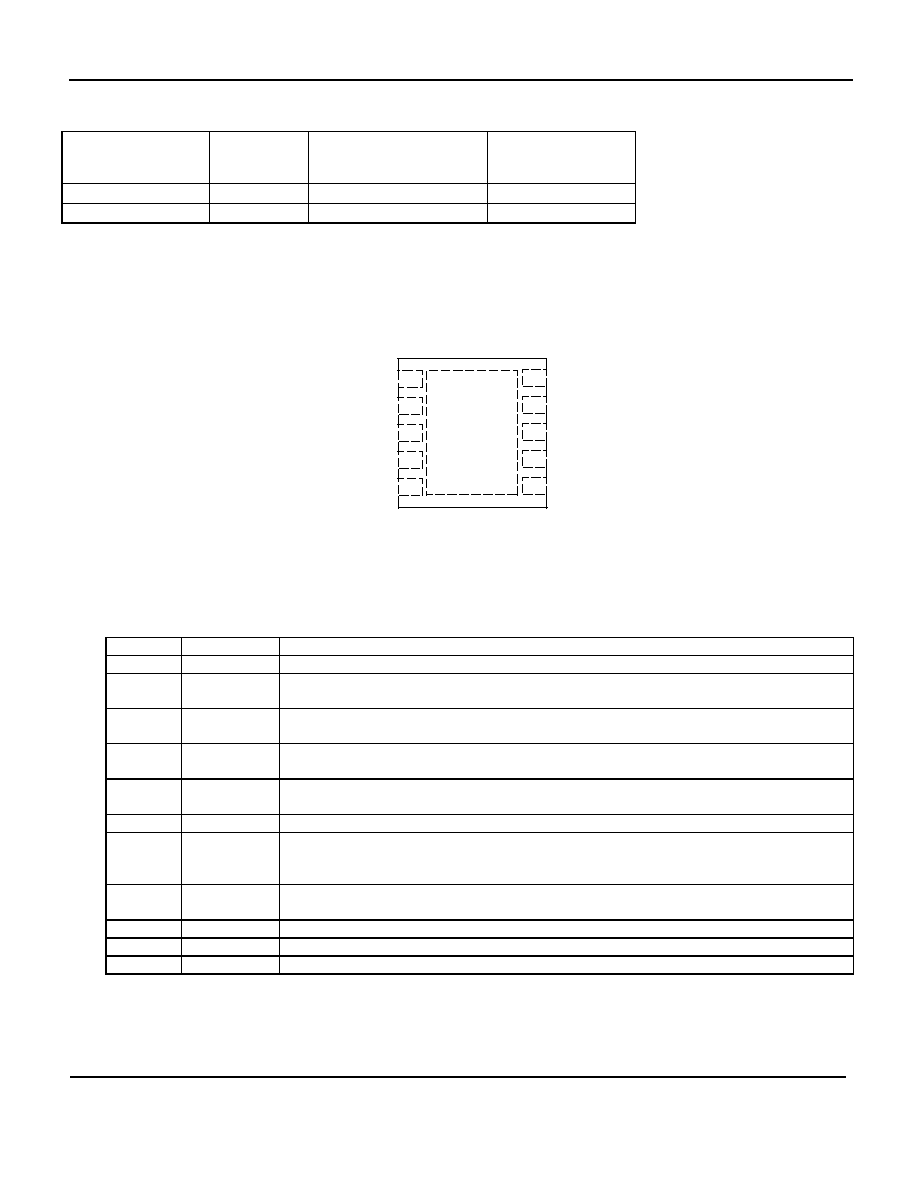
Pin Configuration
1
V
IN
EN1
EN2
LOWQ
BYP
10 V
OUT1
V
OUT2
POR
SET
GND
9
8
7
6
2
3
4
5
MIC5312-xxBML (3x3)
Pin Description
Fixed
Pin Name
Pin Function
1 V
IN
Supply Input. (V
IN1
and V
IN2
are internally tied together)
2
EN1
Enable Input (regulator 1). Active High Input. Logic High = On; Logic Low = Off;
Do not leave floating
3
EN2
Enable Input (regulator 2). Active High Input. Logic High = On; Logic Low = Off;
Do not leave floating
4
LowQTM
LowQTM Mode. Active Low Input. Logic High = Full Power Mode; Logic Low = Light
Load Mode; Do not leave floating.
5
BYP
Reference Bypass: Connect external 0.01µF to GND to reduce output noise. May
be left open.
6 GND
Ground.
7
SET
Delay Set Input: Connect external capacitor to GND to set the internal delay for the
POR output. When left open, there is no delay. This pin cannot be grounded. Delay
= 1µs/1pF
8
POR
Power-On Reset Output: Open-drain output. Active low indicates an output
undervoltage condition on either regulator 1 or regulator 2 when device is enabled.
9 V
OUT
2
Output of regulator 2
10 V
OUT
1
Output of regulator 1
EP
GND
Ground. Internally connected to the Exposed Pad.

Micrel, Inc.
MIC5312
February 2005
3
M9999-021105
(408) 955-1690
Absolute Maximum Ratings
(1)
Supply Input Voltage (V
IN
).............................. 0V to 6V
Enable Input Voltage (V
EN
)............................. 0V to 6V
LowQTM Input Voltage (V
LowQTM
)...................... 0V to 6V
Power Dissipation (P
D
) ..................Internally Limited
(3)
Junction Temperature ....................... -40∞C to +125∞C
Lead Temperature (soldering, 5sec.) .................260∞C
Storage Temperature (T
s
) ................. -65∞C to +150∞C
Operating Ratings
(2)
Supply Input Voltage (V
IN
)..........................2.5V to 5.5V
Enable Input Voltage (EN1/EN2/LowQTM) ...... 0V to V
IN
Junction Temperature (T
J
) .................. -40∞C to +125∞C
Package Thermal Resistance
MLF-10
(
JA
) ................................................. 63∞C/W
Electrical Characteristics (Full Power Mode)
V
IN
= V
OUT
+ 1.0V for higher output of the regulator pair; LowQTM = V
IN
; C
OUT
= 2.2µF, I
OUT
= 100µA; T
J
= 25∞C,
bold
values indicate -40∞C to +125, unless noted.
Parameter Conditions
Min
Typ
Max
Units
Variation from nominal V
OUT
-1.0
+1.0
%
Output Voltage Accuracy
Variation from nominal V
OUT
; -40∞C to +125∞C
-2.0 +2.0
%
Line Regulation
V
IN
= V
OUT
+1V to 5.5V
0.02
0.3
0.6
%/V
Load Regulation
I
OUT
= 100
µ
A to 150mA
I
OUT
= 100
µ
A to 300mA
0.35
0.7
1.0
1.5
%
%
Dropout Voltage
I
OUT
= 150mA
I
OUT
= 300mA
60
120
240
mV
mV
Ground Pin Current
I
OUT
1 = I
OUT
2 = 100µA to 300mA
28
45
50
µA
µA
Ground Pin Current in
Shutdown
V
EN
< 0.2V
0.1
µA
Ripple Rejection
f = up to 1kHz; C
OUT
= 2.2
µ
F ceramic; C
BYP
= 10nF
f = 1kHz ≠ 20kHz; C
OUT
= 2.2
µ
F ceramic; C
BYP
= 10nF
65
35
dB
dB
Current Limit
V
OUT
= 0V (Both Regulators)
350 450 700 mA
Output Voltage Noise
C
OUT
= 2.2
µ
F, C
BYP
= 0.01µF, 10Hz to 100kHz
45 µVrms
Enable and LowQTM Input (EN1/EN2/LowQTM)
Logic Low
0.2
V
Enable Input Voltage
Logic High
1.0
V
V
IL
< 0.2V
0.1
1
µA
Enable Input Current
V
IH
> 1.0V
0.1
1
µA
Turn-on Time
C
OUT
= 2.2µF; C
BYP
= 0.01µF
300
500
µs
Light Load Response
Into Light Load
50
µs
Response Time
(4)
Out of Light Load
50
µs
POR Output
Low Threshold, % of V
OUT
(Flag ON)
90
%
VTH
High Threshold, % of V
OUT
(Flag OFF)
97
%
VOL
POR Output Logic Low Voltage; I
L
= 250µA
0.01
0.1 V
IPOR
Flag Leakage Current, Flag OFF
≠1 0.01 +1
µA
SET INPUT
SET Pin Current Source
V
SET
= 0V
0.75
1.25
1.75
µA
SET Pin Threshold Voltage
1.25
V
Micrel, Inc.
MIC5312
February 2005
4
M9999-021105
(408) 955-1690
Electrical Characteristics (LowQTM Mode)
V
IN
= V
OUT
+ 1.0V for higher output of the regulator pair; LowQTM = 0V; C
OUT
= 2.2µF, I
OUT
= 100µA; T
J
= 25∞C,
bold
values indicate -40∞C to +125∞C, unless noted.
Parameter Conditions
Min
Typ
Max
Units
Output Voltage Accuracy
Variation from nominal V
OUT
-2.0
-3.0
+2.0
+3.0
%
%
Line Regulation
V
IN
= V
OUT
+1V to 5.5V
0.02
0.3
0.6
%/V
Load Regulation
I
OUT
= 100
µ
A to 10mA
0.1
0.5
%
Dropout Voltage
I
OUT
= 10mA
100
200
mV
Ground Pin Current
Both outputs enabled
7
10
12
µA
µA
Ground Pin Current in
Shutdown
V
EN
< 0.2V
0.01
1.0
µA
Ripple Rejection
f = up to 1kHz; C
OUT
= 2.2µF ceramic; C
BYP
= 10nF
f = 1kHz ≠ 20kHz; C
OUT
= 2.2
µ
F ceramic; C
BYP
= 10nF
45
30
dB
dB
Current Limit
V
OUT
= 0V (Both regulators)
40
75
150
mA
Notes:
1. Exceeding the absolute maximum rating may damage the device.
2. The device is not guaranteed to function outside its operating rating.
3. The maximum allowable power dissipation of any T
A
(ambient temperature) is P
D(max)
= T
J(max)
≠ T
A
/
JA
. Exceeding the maximum
allowable power dissipation will result in excessive die temperature, and the regulator will go into thermal shutdown.
4. Response time defined as the minimum hold-off time after the LowQTM command before applying load transients.
Micrel, Inc.
MIC5312
February 2005
5
M9999-021105
(408) 955-1690
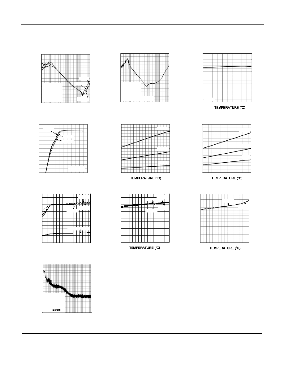
Typical Characteristics
0
10
20
30
40
50
60
70
80
90
PSR
R
(
d
B)
FREQUENCY (Hz)
Ripple Rejection
vs. I
LOAD
(Normal Mode)
150mA
50mA
300mA
10
100
1k
10k
1M
100k
V
OUT
=1.85V
IN
=V
OUT
+1V
=
C
BYP
= 10nF
V
C
OUT
2.2µF
0
10
20
30
40
50
60
70
80
90
PSR
R
(
d
B)
FREQUENCY (Hz)
Ripple Rejection
LowQ Mode
10
100
1k
10k
1M
100k
V
OUT
=1.85V
.
V
IN
=V
OUT
+1V
I
LOAD
=10mA
C
OUT
= 2.2 µF Ceramic
2.3
2.35
2.4
2.45
2.5
2.55
2.6
2.65
2.7
0
25
50
75
100
125
OU
TPU
T
VOL
T
AGE (
V
)
Output Voltage
vs. Temperature
100µA
0
0.5
1
1.5
2
2.5
3
0
1
2
3
4
5
6
OU
TPU
T
VOL
T
AGE (
V
)
SUPPLY VOLTAGE (V)
Dropout Characteristics
100mA
150mA
300mA
V
OUT
=2.6V
0
20
40
60
80
100
120
140
160
-40 -20 0 20 40 60 80 100 120
DROPOUT VOLTAGE (
m
V)
Dropout vs.
Temperature (Normal Mode)
50mA
150mA
300mA
0
20
40
60
80
100
120
140
-40 -20 0 20 40 60 80 100 120
DROPOUT VOLTAGE (
m
V)
Dropout vs.
Temperature (LowQ Mode)
3mA
6mA
10mA
0
5
10
15
20
25
30
35
1.3 1.8 2.3 2.8 3.3 3.8 4.3 4.8 5.3
GROUND CURRE
NT (µA
)
SUPPLY VOLTAGE (V)
Ground Current
100mA
150mA
300mA
10mA LowQTM
vs. Supply Voltage
0
5
10
15
20
25
30
35
-40 -20 0 20 40 60 80 100 120
GROUND CURRENT
(
µ
A)
Ground Current
100mA
150mA
300mA
50mA
vs. Temperature
0
1
2
3
4
5
6
7
8
9
-40 -20 0 20 40 60 80 100 120
GROUND CURRE
NT (µA
)
Ground Current
vs. Temperature (LowQ Mode)
100µA
10mA
0.001
0.01
0.1
1
NOISE (µV/rootHz
)
FREQUENCY (Hz)
Output Noise
Spectral Density
10 100 1k
10k 100k 1M 10M
V
IN
= 4.45V
C
OUT
= 2.2 µF
C
BYP
= 0.01µF
V
OUT
= 1.8V
R
OUT