 | –≠–ª–µ–∫—Ç—Ä–æ–Ω–Ω—ã–π –∫–æ–º–ø–æ–Ω–µ–Ω—Ç: MIC5400 | –°–∫–∞—á–∞—Ç—å:  PDF PDF  ZIP ZIP |
November 2002
1
MIC5400
MIC5400
Micrel
MIC5400
Dual, 8-Output, 14-Bit LED Video Display Driver
General Description
The MIC5400 consists of 2 banks of 8 LED driver outputs,
each output capable of sinking up to 30mA. Each bank is
intended to drive 8 LED pixels of the same color. Most
applications will use the MIC5400 to drive pixel clusters of 4
LEDs (RRGB.) Typically two red LEDs are used for every one
green and blue to compensate for red LED brightness.
A single external resistor sets maximum drive current. Use of
an external resistor allows different color LED banks to be
biased to the same intensity. Brightness control is digitally
programmed through the serial interface. Coarse Brightness
Control is determined by two 4-bit DACs, one for each driver
bank, limiting the full-scale output to a fraction of the maxi-
mum value. Additionally, each output has Fine Brightness
Control using 10-bit resolution PWM.
Groups of drivers can be cascaded in Daisy Chain fashion.
Open circuit output faults are detected and can be read back
from the internal Status register.
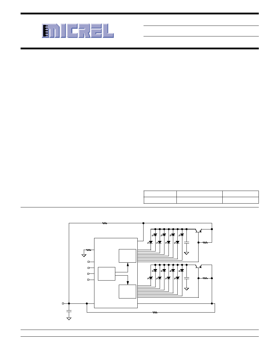
Typical Application
SHFTCLK
VDDA
VDDB
VDD
SHIFTIN
SHIFTOUT
LOAD
0.01µF
2.2µF
2.2µF
Output A
Logic
Control and
SRegister
Output B
BD_A
BD_B
R
SET
330Ω
330Ω
MIC5400
V
DD
R
SC
R
SC
BCP69
BCP69
Features
∑ 2 banks of 8 outputs
∑ Output characteristics:
∑ Current sink: 30mA
≠ Programmable brightness control
∑ Coarse: 4-bit resolution DAC
∑ Fine: 10-bit resolution PWM
≠ Resistor sets maximum LED current to compensate
variation in LEDs
≠ Current limit on each output
∑ Full protection:
≠ Over-temperature shutdown
≠ Watchdog disables output under fault condition
≠ Power-on reset (all LEDs Off)
≠ Soft-start on power up and watchdog recovery
≠ Output open fault detection with status register
readback
∑ Output transitions are staggered to minimize supply
transients
Applications
∑ Outdoor video screen
∑ Large LED display
Ordering Information
Part Number
Junction Temp. Range
Package
MIC5400BWM
≠40
∞
C to +85
∞
C
28-Pin Wide SOIC
Micrel, Inc. ∑ 1849 Fortune Drive ∑ San Jose, CA 95131 ∑ USA ∑ tel + 1 (408) 944-0800 ∑ fax + 1 (408) 944-0970 ∑ http://www.micrel.com

MIC5400
Micrel
MIC5400
2
November 2002
Pin Description
Pin Number
Pin Name
Pin Function
Pin
Name
Function
1,2,3,4
A4,A3,A2,A1
Current Sink pins to be connected to LED cathodes
5
LOAD
If this pin is Low, the device acts as a shift register. When this pin is High,
only the first falling edge of the clock transfers data from the Shift-Register to
the Parallel Register. The next rising edge transfers data from the Status
Register to the Shift Register
6
SHFTCLK
Shift-register Clock Input
7
VDD
Positive Supply Voltage
8,22
GND
Ground
9
SHIFTIN
Shift-register Data Input
10
SHIFTOUT
Shift-register Data Output
11,12,13,14
B1,B2,B3,B4
Current Sink pins to be connected to LED cathodes
15,16,17,18
B5,B6,B7,B8
Current Sink pins to be connected to LED cathodes
19
VDDB
Analog Power source pins which provide current sense points for Channel A
and Channel B PNP emitter currents, independently.
20
BD_B
Base Drive Outputs for external PNP transistors. Feedback Loop compensa-
tion requires one external capacitor at each PNP transistor collector.
21
REF
Reference current output. Must be connected to an external resistor to set
the maximum current for the current sink outputs.
23
BD_A
Base Drive Outputs for external PNP transistors. Feedback Loop compensa-
tion requires one external capacitor at each PNP transistor collector.
24
VDDA
Analog Power source pins which provide current sense points for Channel A
and Channel B PNP emitter currents, independently.
25,26,27,28
A8,A7,A6,A5
Current Sink pins to be connected to LED cathodes
Pin Configuration
1
A4
A3
A2
A1
LOAD
SHFTCLK
VDD
GND
SHIFTIN
SHIFTOUT
28 A5
A6
A7
A8
VDDA
BD_A
GND
IREF
BD_B
VDDB
27
26
25
24
23
22
21
20
19
2
3
4
5
6
7
8
9
10
B1
B8
18
11
B2
B7
17
12
B3
B6
16
13
B4
B5
15
14
28-Lead SOIC
November 2002
3
MIC5400
MIC5400
Micrel
Absolute Maximum Ratings
(Note 1)
Supply Voltage .............................................................. +7V
Input Voltage ....................................... ≠0.3V to V
CC
+ 0.3V
Base Drive Voltage ....................................................... +7V
Output Sink Current (per output) ................................ 35mA
Lead Temperature (soldering, 5 sec) ........................ 260
∞
C
Junction Temperature (T
J
)(max) ............................... 125
∞
C
Operating Ratings
(Note 2)
Supply Voltage (V
CC
) ................................ +4.75V to +5.5V
Junction Temperature (T
J
) ....................... ≠40
∞
C to +125
∞
C
Package Thermal Resistance
SOIC (
JC
) .......................................................... 28
∞
C/W
SOIC (
JA
) ......................................................... 100
∞
C/W
DC Electrical Characteristics
V
DD
= 4.75V to 5.5 V, T
A
= 25
∞
C, bold values indicate ≠40
∞
C
T
A
+85
∞
C. R
BIAS
= 500
. Applies to all channels unless noted.
Symbol
Parameter
Condition
Min
Typ
Max
Units
I
OUT
Output Sink Current
26
35
mA
I
OUT
Output Current Matching
7
%
I
OUT(OFF)
Output Off Leakage
V
OUT
= 5V
≠1
1
µ
A
I
DD
Supply Current
V
DD
= 5.5V
0
2
mA
I
B
PNP Base Drive Current
V
BD
= 4V
7
50
mA
V
REF
Reference Output Voltage
I
REF
= ≠4mA
1.9
2.1
V
V
IH
Logic 1 Input Threshold
2.2
V
V
IL
Logic 0 Input Threshold
0.8
V
V
OH
Logic 1 Output Level
I
LOAD
= 1mA
2.4
V
V
OL
Logic 0 Output Level
I
LOAD
= 1mA
0.4
V
T
SHUTDOWN
Thermal Shutdown Temperature
165
∞
C
AC Electrical Characteristics
V
DD
= 4.75V to 5.5V, T
A
= 25
∞
C, bold values indicate ≠40
∞
C
T
A
+85
∞
C. R
BIAS
= 500
. Applies to all channels unless noted
Symbol
Parameter
Conditions
Min
Typ
Max
Units
f
SHIFT
Shift Frequency
15
MHz
t
SET-DATA
Set Up Time for Data In
Note 5
7
ns
t
HOLD-DATA
Hold Time for Data In
Note 5
13
ns
t
SET-LOAD
Set Up Time for Load
Note 5
20
ns
t
HOLD-LOAD
Hold Time for Load
Note 5
13
ns
I
OUT(tr)
Rise Time I
OUT
Note 4, 5
125
ns
I
OUT(ttf)
Fall Time I
OUT
Note 4, 5
50
ns
t
D-SHIFT
Clock to Shift Out Delay
Rise and Fall, 50% C
LOAD
= 30pF, Note 5
23
ns
t
r,f-OUT
Shift Out Rise and Fall Time
10% to 90%; C
LOAD
=30pF, Note 5
10
ns
t
WD-TIMEOUT
Watch Dog Timeout Delay
No Shiftclock
25
200
µ
s
t
r,f[in]
Logic Input Rise and Fall Times
10
ns
Note 1.
Exceeding the absolute maximum rating may damage the device.
Note 2.
The device is not guaranteed to function outside its operating rating.
Note 3.
Devices are ESD sensitive. Handling precautions recommended. Human body model, 1.5k in series with 100pF.
Note 4.
Test circuit shown in Figure 1.
Note 5.
Guaranteed by design; not production tested.

MIC5400
Micrel
MIC5400
4
November 2002
Test Circuit
V
OUT
to FET Probe (C < 1.5pF)
75
V
DD
= 5V
OUT
N
Controller
Device
Under Test
Figure 1. AC Output Test Circuit
Timing Diagrams
SHFTCLK
LOAD
D
N-1
D
N
D
N
D
N
S
N
Shifting
Shifting
S
N
S
N
S
N
S
N+1
Control Register Contents
Shift Register Contents
Status Register Contents
Figure 2. MIC5400 Timing Diagram
Linearity
5
10
15
20
25
30
35
40
45
1.5 2 2.5 3 3.5 4 4.5 5 5.5
I
OUT
( mA )
I
REF
(mA)
Typical Global Full Scale Linearity
(any output)
Linear Operating Region
(Recommended)
Non-Linear
Operation
T
J
= 25
∞
Figure 3. Typical Global Full Scale Linearity
November 2002
5
MIC5400
MIC5400
Micrel
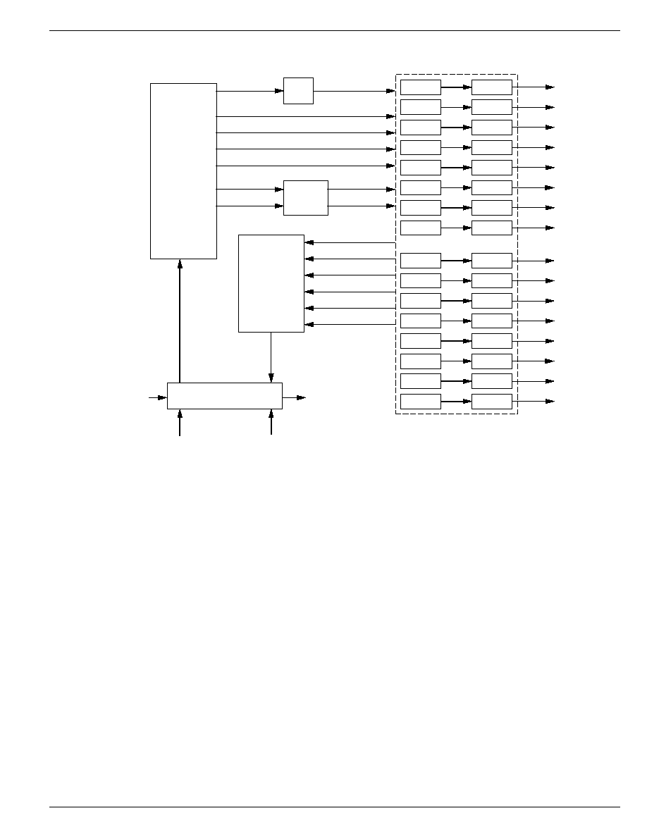
Functional Diagram
PWM
Select
PWM 1
Out 1A
36 Bit Shift Register
PWM Select (3 Bits)
PWM Data A (10 Bits)
PWM Data B (10 Bits)
Watchdog Enable (1 Bits)
Divisor (4 Bits)
Data and
Control Register
(36 bits)
Status Register
(36 bits)
2X4-bit
Brightness
DAC
DAC A (4 Bits)
DAC B (4 Bits)
IREF A
Select 1 of 8 in Bank A/B
IREF B
Status A (8 Bits)
Status B (8 Bits)
Watchdog Status (1 Bits)
Thermal Status (1 Bits)
Mask Rev. (3 Bits)
Fixed Pattern (15 Bits)
PWM 2
Out 2A
PWM 3
Out 3A
PWM 4
Out 4A
PWM 5
Out 5A
PWM 6
Out 6A
PWM 7
Out 7A
PWM 8
Out 8A
PWM 1
SHFTCLK
SHIFTIN
LOAD
SHIFTOUT
Out 1B
PWM 2
Out 2B
PWM 3
Out 3B
PWM 4
Out 4B
PWM 5
Out 5B
PWM 6
Out 6B
PWM 7
Out 7B
PWM 8
Out 8B
MIC5400 Functional Diagram