 | –≠–ª–µ–∫—Ç—Ä–æ–Ω–Ω—ã–π –∫–æ–º–ø–æ–Ω–µ–Ω—Ç: MIC59P60 | –°–∫–∞—á–∞—Ç—å:  PDF PDF  ZIP ZIP |
January 2000
1
MIC59P60
MIC59P60
Micrel
Ordering Information
Part Number
Temperature Range
Package
MIC59P60BN
≠40
∞
C to +85
∞
C
20-Pin Plastic DIP
MIC59P60BV
≠40
∞
C to +85
∞
C
20-Pin PLCC
MIC59P60BWM
≠40
∞
C to +85
∞
C
20-Pin Wide SOIC
3
4
5
11
19
18
17
16
15
13
12
7
6
8
9
2
10
1
14
20
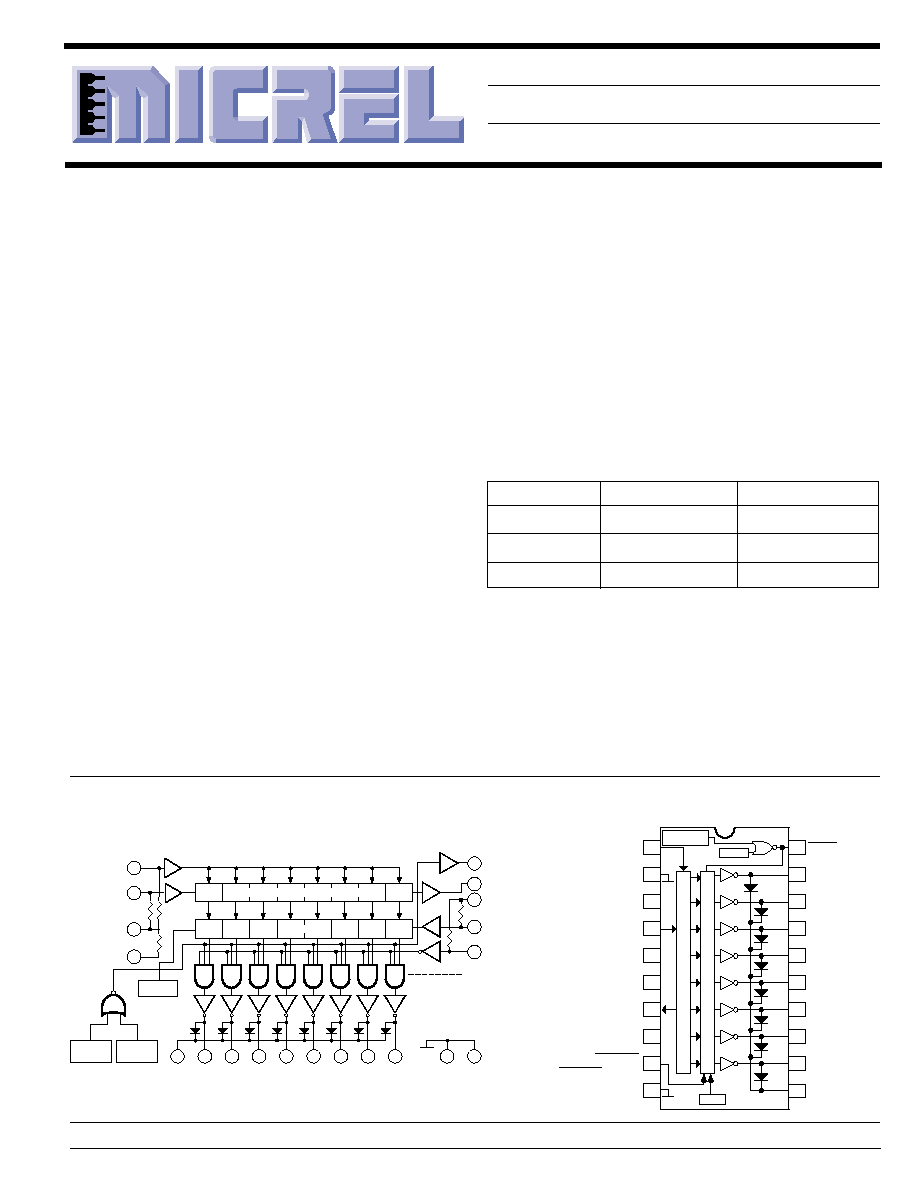
CLOCK
SERIAL
DATA IN
VSS
CLEAR
UVLO
THERMAL
SHUTDOWN
ILIMIT
K
OUT 1 OUT 2 OUT 3 OUT 4 OUT 5 OUT 6 OUT 7 OUT 8
SUB
VEE
MOS
BIPOLAR
OUTPUT
ENABLE/RESET
STROBE
VDD
SERIAL DATA OUT
FLAG
8-BIT SERIAL≠PARALLEL SHIFT REGISTER
LATCHES
Features
∑ 3.3 MHz Minimum Data-Input Rate
∑ Output Current Shutdown (500mA Typical)
∑ Under Voltage Lockout
∑ Thermal Shutdown
∑ Output Fault Flag
∑ CMOS, PMOS, NMOS, and TTL Compatible
∑ Internal Pull-Up/Pull-Down Resistors
∑ Low Power CMOS Logic and Latches
∑ High Voltage Current Sink Outputs
∑ Output Transient-Protection Diodes
∑ Single or Split Supply Operation
UVLO
I LIMIT
THERMAL
SHUTDOWN
10
9
8
7
6
5
4
3
2
1
SUB
SUB
SHIFT REGISTER
LATCHES
20
19
18
17
16
15
14
13
12
11
CLEAR
VEE
CLOCK
SERIAL DATA IN
VSS
VDD
SERIAL DATA OUT
STROBE
ENABLE/RESET
VEE
OUTPUT
FLAG
OUTPUT 1
OUTPUT 2
OUTPUT 3
OUTPUT 4
OUTPUT 5
OUTPUT 6
OUTPUT 7
OUTPUT 8
K
Pin Configuration
(DIP and SOIC)
MIC59P60
8-Bit Serial-Input Protected Latched Driver
General Description
The MIC59P60 serial-input latched driver is a high-voltage
(80V), high-current (500mA) integrated circuit comprised of
eight CMOS data latches, a bipolar Darlington transistor
driver for each latch, and CMOS control circuitry for the
common CLEAR, STROBE, CLOCK, SERIAL DATA INPUT,
and OUTPUT ENABLE functions. Similar to the MIC5842,
additional protection circuitry supplied on this device includes
thermal shutdown, under voltage lockout (UVLO), and over-
current shutdown.
The bipolar/CMOS combination provides an extremely low-
power latch with maximum interface flexibility. The MIC59P60
has open-collector outputs capable of sinking 500mA and
integral diodes for inductive load transient suppression with
a minimum output breakdown voltage rating of 80V (50V
sustaining). The drivers can be operated with a split supply,
where the negative supply is down to ≠20V and may be
paralleled for higher load current capability.
Using a 5V logic supply, the MIC59P60 will typically operate
at better than 5MHz. With a 12V logic supply, significantly
higher speeds are obtained. The CMOS inputs are compat-
ible with standard CMOS, PMOS, and NMOS circuits. TTL
circuits may require pull-up resistors. By using the serial data
output, drivers may be cascaded for interface applications
requiring additional drive lines.
Each of these eight outputs has an independent over current
shutdown of 500 mA. Upon over-current shutdown, the
affected channel will turn OFF and the flag will go low until V
DD
is cycled or the ENABLE/RESET pin is pulsed high. Current
pulses less than 2
µ
s will not activate current shutdown.
Temperatures above 165
∞
C will shut down the device and
activate the error flag. The UVLO circuit prevents operation
at low V
DD
; hysteresis of 0.5V is provided.
Functional Diagram
Micrel, Inc. ∑ 1849 Fortune Drive ∑ San Jose, CA 95131 ∑ USA ∑ tel + 1 (408) 944-0800 ∑ fax + 1 (408) 944-0970 ∑ http://www.micrel.com
MIC59P60
2
January 2000
MIC59P60
Micrel
Pin Description
Pin
Name
Description
1
CLEAR
Sets All Latches OFF (open).
2,10
V
EE
Output Ground (Substrate). Most negative voltage in the system connects
here.
3
CLOCK
Serial Data Clock. A CLEAR must also be clocked into the latches.
4
SERIAL DATA IN
Serial Data Input pin.
5
V
SS
Logic reference (Ground) pin.
6
V
DD
Logic Positive Supply voltage.
7
SERIAL DATA OUT
Serial Data Output pin. (Flow through).
8
STROBE
Output Strobe pin. Loads output latches when High. A STROBE is needed
to CLEAR latches.
9
OUTPUT ENABLE/RESET
When Low, Outputs are active. When High, device is inactive and reset
from a fault condition. An under voltage condition emulates a high OE/
RESET input.
11
K
Transient suppression diode's cathode common pin.
12--19
OUTPUT N
Open Collector outputs 8 through 1.
20
FLAG
Error Flag. Flag is Low upon Overcurrent Fault or Overtemperature fault.
OUTPUT ENABLE/RESET must be pulled high to reset the flag and fault
condition.
Absolute Maximum Ratings
V
SS
= 0; T
A
= 25
∞
C
Output Voltage (V
CE
) .................................................... 80V
Output Voltage (V
CE(SUS)
) ............................... 50V, Note 1
V
DD
with Reference to V
SS
........................................... 15V
V
DD
with Reference to V
EE
........................................... 25V
Emitter Supply Voltage (V
EE
) ...................................... ≠20V
Input Voltage (V
IN
) ............................... ≠0.3V to V
DD
+0.3V
Protected Current ............................................ 1.5A, Note 2
Power Dissipation (P
D
)
Plastic DIP (N) ......................................................... 2.0W
Derate above T
A
= +25
∞
C ............................ 20mW/
∞
C
PLCC (V) ................................................................. 1.4W
Derate above T
A
= +25
∞
C ............................ 14mW/
∞
C
Wide SOIC (WM) .................................................... 1.2W
Derate above T
A
= +25
∞
C ............................ 12mW/
∞
C
Operating Temperature (T
A
)
Plastic DIP (N), PLCC (V), SOIC (WM) .. ≠40
∞
C to +85
∞
C
Storage Temperature (T
S
) ....................... ≠65
∞
C to +150
∞
C
Junction Temperature (T
J
) ...................................... +150
∞
C
ESD ......................................................................... Note 3
Note 1:
For inductive load applications.
Note 2:
Each channel. V
EE
connection must be designed to minimize
inductance and resistance.
Note 3:
Devices are input-static protected but can be damaged by
extremetly high static charges.
PLCC Pin
Configuration
CLOCK
SERIAL
DATA IN
DD
V
SS
V
STROBE
OUTPUT
ENABLE
DD
V
SS
V
SUB
N
OUT
K
EE
V
3K
1
2
3
4
12
13
11
20
19
18
14
15
16
17
9
10
5
6
7
8
OUT 1
OUT 2
OUT 3
OUT 4
OUT 5
OUT 6
OUT 7
OUT 8
K
SERIAL DATA OUT
VSS
SERIAL DATA IN
STROBE
CLEAR
OE/RESET
VDD
FLAG
V
EE
MIC59P60BV
CLOCK
V
EE
Typical Inputs
Typical Output Driver

January 2000
3
MIC59P60
MIC59P60
Micrel
Electrical Characteristics
V
DD
= 5V, V
SS
= V
EE
= 0V; T
A
= +25
∞
C; unless noted.
Limits
Characteristic
Symbol
Test Conditions
Min.
Typ.
Max.
Unit
Output Leakage Current
I
CEX
V
OUT
= 80V
50
µ
A
V
OUT
= 80V, T
A
= +70
∞
C
100
Collector-Emitter
V
CE(SAT)
I
OUT
= 100mA
0.9
1.1
V
Saturation Voltage
I
OUT
= 200mA
1.1
1.3
I
OUT
= 350mA
1.3
1.6
Collector-Emitter
V
CE(SUS)
I
OUT
= 350mA, L = 2mH
50
V
Sustaining Voltage
Input Voltage
V
IN(0)
1.0
V
V
IN(1)
V
DD
= 12V
10.5
V
V
DD
= 10V
8.5
V
DD
= 5.0V, Note 4
3.5
Input Resistance
R
IN
V
DD
= 12V
50
200
k
V
DD
= 10V
50
300
V
DD
= 5.0V
50
600
Flag Output Current
I
OL
V
OL
= 0.4V
15
mA
Flag Output Leakage
I
OH
V
OH
= 12.0V
50
nA
Supply Current
I
DD(ON)
All Drivers ON, V
DD
= 12V
6.4
10.0
mA
All Drivers ON, V
DD
= 10V
6.0
9.0
All Drivers ON, V
DD
= 5.0V
4.6
7.5
I
DD (1 OUTPUT)
One Driver ON, All others OFF, V
DD
= 12V
3.1
4.5
mA
One Driver ON, All others OFF, V
DD
= 10V
2.9
4.5
One Driver ON, All others OFF, V
DD
= 5V
2.3
3.6
I
DD(OFF)
All Drivers OFF, V
DD
= 12V
2.6
4.2
mA
All Drivers OFF, V
DD
= 10V
2.4
3.6
All Drivers OFF, V
DD
= 5.0V
1.9
3.0
Clamp Diode
I
R
V
R
= 80V
50
µ
A
Leakage Current
Clamp Diode
V
F
I
F
= 350mA
1.7
2.0
V
Forward Voltage
Over Current
I
LIM
500
mA
Shutdown Threshold
Start Up Voltage
V
SU
Note 5
3.5
4.0
4.5
V
Minimum Supply (V
DD
)
V
DD MIN
3.0
3.5
4.0
V
Thermal Shutdown
165
∞
C
Thermal Shutdown Hysteresis
10
∞
C
Note 4: Operation of these devices with standard TTL or DTL may require the use of appropriate pull-up resistors to insure a minimum logic "1".
Note 5: Undervoltage lockout is guaranteed to release device at no more than 4.5V, and disable the device at no less than 3.0V
MIC59P60
4
January 2000
MIC59P60
Micrel
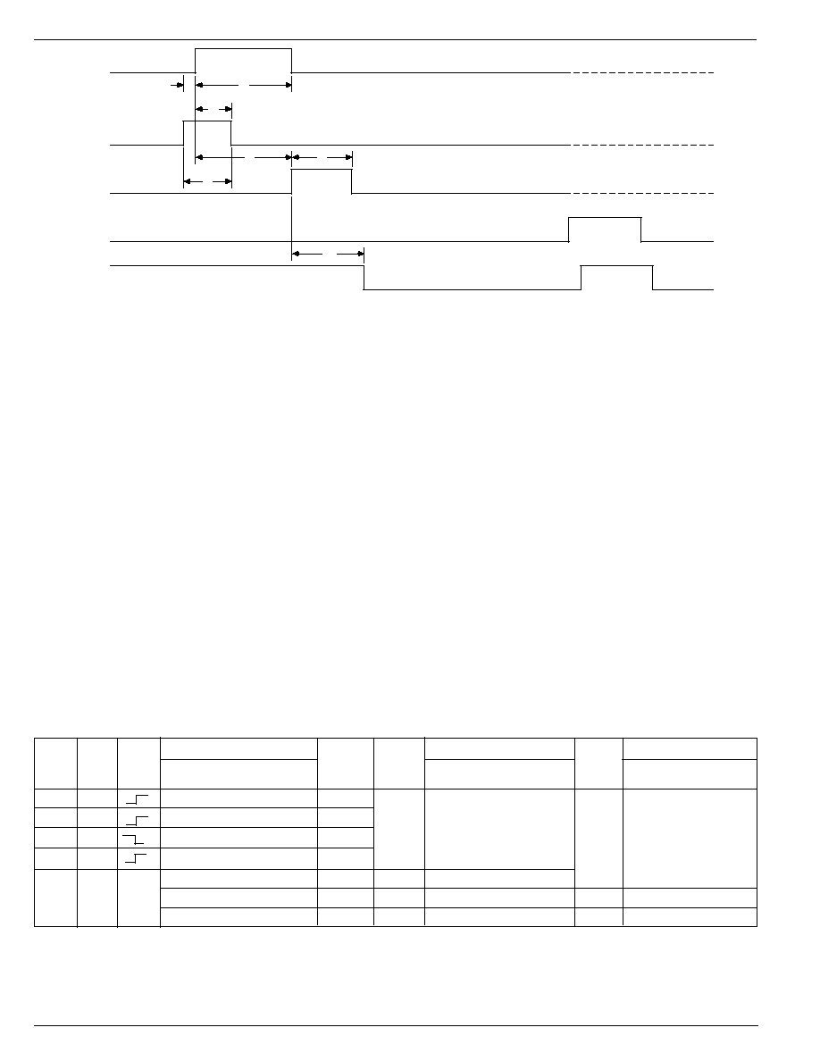
Timing Conditions
(T
A
= +25
∞
C, Logic Levels are V
DD
and V
SS,
V
DD
= 5V)
A. Typical Data Active Time Before Clock Pulse (Data Set-Up Time) ........................................................................... 75 ns
B. Minimum Data Active Time After Clock Pulse (Data Hold Time) .............................................................................. 75 ns
C. Minimum Data Pulse Width ..................................................................................................................................... 150 ns
D. Minimum Clock Pulse Width .................................................................................................................................... 150 ns
E. Minimum Time Between Clock Activation and Strobe ............................................................................................. 300 ns
F. Minimum Strobe Pulse Width ................................................................................................................................... 100 ns
G. Typical Time Between Strobe Activation and Output Transition ............................................................................. 500 ns
SERIAL DATA present at the input is transferred to the shift register on the logic "0" to logic "1" transition of the CLOCK input
pulse. On succeeding CLOCK pulses, the registers shift data information towards the SERIAL DATA OUTPUT. The SERIAL
DATA must appear at the input prior to the rising edge of the CLOCK input waveform. Holding CLEAR high results in a data
logic "0" being clocked into the shift register, turning off respective channels.
Information present at any register is transferred to its respective latch when the STROBE is high (serial-to-parallel conversion).
The latches will continue to accept new data as long as the STROBE is held high. Applications where the latches are bypassed
(STROBE tied high) will require that the ENABLE input be high to prevent invalid output states.
When the ENABLE input is high, all of the output buffers are disabled (OFF) without affecting information stored in the latches
or shift register. With the ENABLE input low, the outputs are controlled by the state of the latches. A positive OE/RESET pulse
resets the FLAG and the output after a current shutdown fault. Over-temperature faults are not latched and require no reset
pulse.
CLOCK
DATA IN
STROBE
OUTPUT
ENABLE
D
B
A
E
C
G
OUTN
F
MIC59P60 Truth Table
Serial
Shift Register Contents
Serial
Latch Contents
Output Contents
Data
Clear Clock
Data
Strobe
Output
Input
Input Input I
1
I
2
I
3
......
I
8
Output
Input
I
1
I
2
I
3
......
I
8
Enable
I
1
I
2
I
3
...... I
8
H
H
R
1
R
2
......
R
7
R
7
L
L
R
1
R
2
......
R
7
R
7
X
R1
R2
R
3
......
R
8
R
8
H
O
O
O ......
O
L
X
X
X ......
X
X
L
R
1
R
2
R
3
......
R
8
P
1
P
2
P
3
......
P
8
P
8
H
P
1
P
2
P
3
......
P
8
L
P
1
P
2
P
3
......P
8
X
X
X
......
X
H
H
H
H
...... H
L = Low Logic Level
H = High Logic Level
X = Irrelevant
P = Present State
R = Previous State
O = Output OFF

January 2000
5
MIC59P60
MIC59P60
Micrel
Typical Characteristic Curves
0.5
0.6
0.7
0.8
0.9
1
1.1
1.2
1.3
1.4
1.5
≠50
0
50
100
150
SATURATION VOLTAGE (V)
TEMPERATURE (∞C)
Output Saturation
Voltage vs. Temperature
I
L
= 350mA
I
L
= 100mA
V
DD
= 5V to 12V
0.35
0.40
0.45
0.50
0.55
0.60
≠50
0
50
100
150
SHUTDOWN THRESHOLD (A)
TEMPERATURE (∞C)
V
DD
= 5V
V
DD
= 12V
Current Shutdown
Threshold vs. Temperature
0.5
0.6
0.7
0.8
0.9
1
1.1
1.2
1.3
1.4
1.5
-50
0
50
100
150
SATURATION VOLTAGE (V)
TEMPERATURE (∞C)
Output Saturation
Voltage vs. Temperature
VDD = 12V
IL = 350mA
IL = 100mA
0
1
2
3
4
5
6
7
≠50
0
50
100
150
SUPPLY CURRENT (mA)
TEMPERATURE (∞C)
Supply Current
vs. Temperature
ALL OUTPUTS ON
ALL OUTPUTS OFF
V
DD
= 12V
0
2
4
6
8
10
12
14
16
18
20
0.3
0.4
0.5
0.6
0.7
0.8
0.9
CURRENT LIMIT DELAY (µS)
OUTPUT CURRENT (A)
Current Shutdown
Delay vs. Output Current
V
DD
= 12V
V
DD
= 5V
0
1
2
3
4
5
≠50
0
50
100
150
SUPPLY CURRENT (mA)
TEMPERATURE (∞C)
ALL OUTPUTS ON
ALL OUTPUTS OFF
Supply Current
vs. Temperature
V
DD
= 5V