June 1999
1
MIC6211
MIC6211
Micrel
MIC6211
IttyBittyTM Operational Amplifier
Preliminary Information
General Description
The MIC6211 IttyBittyTM op amp is a general-purpose, high-
performance, single- or split-supply, operational amplifier in
a space-saving, surface-mount package.
The MIC6211 operates from 4V to 32V, single or differential
(split) supply. The input common-mode range includes ground.
The device features a 2.5MHz unity gain bandwidth, 6V/
µ
s
slew rate, and is internally unity-gain compensated.
Inputs are protected against reverse polarity (input voltage
less than V≠) and ESD (electrostatic discharge). Output is
current limited for both sourcing and sinking. Output short
circuits of unlimited duration are allowed, provided the power
dissipation specification is not exceeded.
The MIC6211 is available in the tiny, 5-lead SOT-23-5 sur-
face-mount package.
Functional Configuration
OUT
V+
IN≠
IN+
1
3
4
5
2
V≠
SOT-23-5 (M5)
Features
∑ 4V to 32V operation
∑ Small footprint package
∑ Unity gain stable
∑ 2.5 MHz unity gain bandwidth
∑ 6V/
µ
s typical slew rate
∑ Short circuit protected
Applications
∑ Analog blocks
∑ Active filtering
Ordering Information
Part Number
Temperature Range
Package
MIC6211BM5
≠40
∞
C to +85
∞
C
SOT-23-5
Pin Description
Pin Number
Pin Name
Pin Function
1
OUT
Amplifier Output
2
V≠
Negative Supply: Negative supply for split supply application or ground for
single supply application.
3
IN+
Noninverting Input
4
IN≠
Inverting Input
5
V+
Positive Supply
Pin Configuration
Part
Identification
OUT
V+
IN≠
IN+
A11
1
3
4
5
2
V≠
Micrel, Inc. ∑ 1849 Fortune Drive ∑ San Jose, CA 95131 ∑ USA ∑ tel + 1 (408) 944-0800 ∑ fax + 1 (408) 944-0970 ∑ http://www.micrel.com

MIC6211
Micrel
MIC6211
2
June 1999
Electrical Characteristics (Differential Supply)
V+ = +15V, V≠ = ≠15V, V
CM
= 0V; R
L
= 2k
; T
A
= 25
∞
C, bold values indicate ≠40
∞
C
T
A
+85
∞
C, T
A
= T
J
; unless noted
Symbol
Parameter
Condition
Min
Typ
Max
Units
V
OS
Input Offset Voltage
2
7
mV
TCV
OS
Average Input Offset Drift
Note 1
7
µ
V/
∞
C
I
B
Input Bias Current
50
250
nA
I
OS
Input Offset Current
8
30
nA
V
CM
Input Voltage Range
+13.5
+13.8
V
≠15.0
≠15.3
V
CMRR
Common Mode Rejection Ratio
V
CM
= +13.5V, ≠15.0V
65
100
dB
PSRR
Power Supply Rejection Ratio
V
S
=
±
2.5V to
±
15V
65
110
dB
A
VOL
Large Signal Voltage Gain
V
O
=
±
10V
25
180
V/mV
V
OUT
Maximum Output Voltage Swing
±
12.5
±
14
V
B
W
Bandwidth
2.5
MHz
S
R
Slew Rate
6
V/
µ
s
I
SC
Output Short Circuit Current
Sourcing or sinking
30
50
mA
I
S
Supply Current
1.3
2.0
mA
Electrical Characteristics (Single Supply)
V+ = +5V, V≠ = 0V, V
CM
= 0.1V; T
A
= 25
∞
C, bold values indicate ≠40
∞
C
T
A
+85
∞
C, T
A
= T
J
; unless noted
Symbol
Parameter
Condition
Min
Typ
Max
Units
V
OS
Input Offset Voltage
2
7
mV
TCV
OS
Average Input Offset Drift
Note 1
7
µ
V/
∞
C
I
B
Input Bias Current
65
250
nA
I
OS
Input Offset Current
8
30
nA
V
CM
Input Voltage Range
+3.5
+3.7
V
0
≠0.3
V
CMRR
Common Mode Rejection Ratio
V
CM
= 0V to 3.5V
45
70
dB
PSRR
Power Supply Rejection Ratio
V
S
=
±
2.5V to
±
15V
65
105
dB
A
VOL
Large Signal Voltage Gain
V
O
= 1.5V to 3.5V, R
L
= 2k
15
170
V/mV
V
OUT
Maximum Output Voltage Swing
R
L
= 10k to GND
+3.8
+4.0
V
R
L
= 10k to +5V
+1.0
+1.2
V
I
SC
Output Short Circuit Current
Sourcing or sinking
20
40
mA
I
S
Supply Current
1.2
1.8
mA
General Note: Devices are ESD protected; however, handling precautions are recommended.
Note 1:
Not production tested.
Absolute Maximum Ratings
Supply Voltage (V
V+
≠ V
V≠
) ............................. 36V or
±
18V
Differential Input Voltage (V
IN+
≠ V
IN≠
) .......................
±
36V
Input Voltage (V
IN+
, V
IN≠
) ..................... (V
V≠
≠ 0.3V) to V
V+
Output Short Circuit Current Duration ...............................
Operating Ratings
Supply Voltage .................................................... 4V to 32V
Ambient Temperature Range ..................... ≠40
∞
C to +85
∞
C
SOT-23-5 Thermal Resistance (
JA
) ..................... 220
∞
C/W
(mounted to printed circuit board)

June 1999
3
MIC6211
MIC6211
Micrel
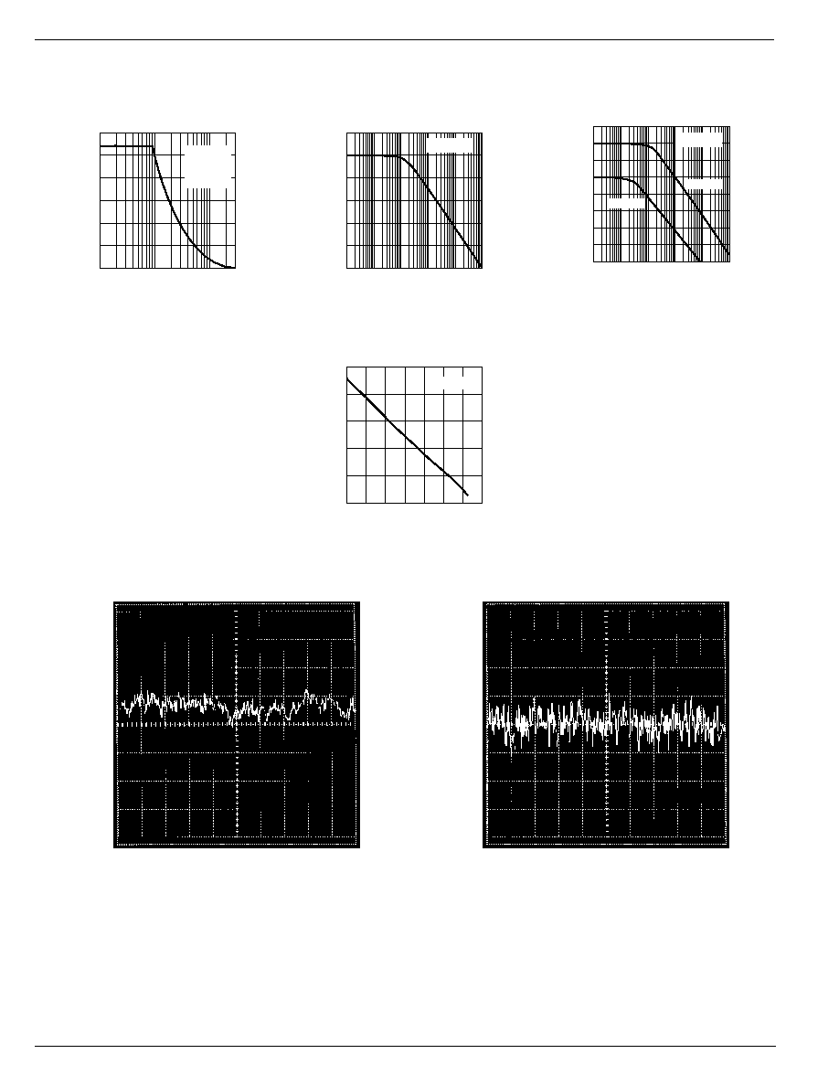
Typical Characteristics
30
40
50
60
70
80
90
-40 -20
0
20
40
60
80 100
INPUT BIAS CURRENT (nA)
TEMPERATURE (
∞
C)
Input Bias Current
vs. Temperature
V
S
= 5V
V
S
=
±
15V
0
5
10
15
20
-40 -20
0
20
40
60
80 100
INPUT OFFSET CURRENT (nA)
TEMPERATURE (
∞
C)
Input Offset Current
vs. Temperature
V
S
=
±
15V
V
S
= 5V
0
0.5
1.0
1.5
0
5
10
15
20
25
30
SUPPLY CURRENT (mA)
SUPPLY VOLTAGE (V)
Supply Current
vs. Supply Voltage
-20
0
20
40
60
80
100
120
0.01
0.1
1
10
100
1,000
10,000
VOLTAGE GAIN (dB)
FREQUENCY (kHz)
Voltage Gain
vs. Frequency
V
S
=
±
15V
-20
-10
0
10
20
30
270
225
180
135
90
45
0.1
1.0
10
VOLTAGE GAIN (dB)
PHASE (
∞
)
FREQUENCY (MHz)
GAIN
PHASE
Gain and Phase
vs. Frequency
V
S
=
±
15V
72
∞
GND
+10V
≠10V
INPUT VOLTAGE OUTPUT VOLTAGE
Large-Signal Transient Response
≠10V
GND
+10V
AV = +1
RL = 2k
CL = 10pF
VS =
±
15V
2
µ
s/DIV
GND
+50mV
≠50mV
INPUT VOLTAGE OUTPUT VOLTAGE
Small-Signal Transient Response
≠50mV
GND
+50mV
AV = +1
RL = 2k
CL = 100pF
VS =
±
15V
500ns/DIV
1.0
1.1
1.2
1.3
1.4
-40 -20
0
20
40
60
80 100
SUPPLY CURRENT (mA)
TEMPERATURE (
∞
C)
Supply Current
vs. Temperature
V
S
=
±
15V
V
S
= 5V