July 1998
1
MIC6251/6252
MIC6251/6252
Micrel
MIC6251/6252
IttyBittyTM GainBlockTM Amplifiers
Final Information
General Description
The MIC6251 and MIC6252 are IttyBittyTM GainBlockTM
amplifiers for use as follows:
MIC6251 ................................ +2, +1, ≠1 gain amplifier
MIC6252 .................................. +0.5, +1 gain amplifier;
average value amplifier
The MIC6251 and MIC6252 amplifiers operate from 4V to
32V. Both can use single or split supplies. These amplifiers
feature internal, well-matched, gain-setting resistors and an
input common-mode range that includes the negative supply
(ground).
The MIC6251/2 is available in the tiny SOT-23-5 surface
mount package.
Features
∑ 4V to 32V operation
∑ Small footprint package
∑ Internally compensated
∑ 2MHz bandwidth
∑ 6V/
µ
s typical slew rate
∑ Short circuit protected
Applications
∑ Analog building blocks
∑ Summing amplifier
∑ Gain block
Ordering Information
Part Number
Marking
Temperature
Range Package
MIC6251BM5
A51
≠40
∞
C to +85
∞
C
SOT-23-5
MIC6252BM5
A52
≠40
∞
C to +85
∞
C
SOT-23-5
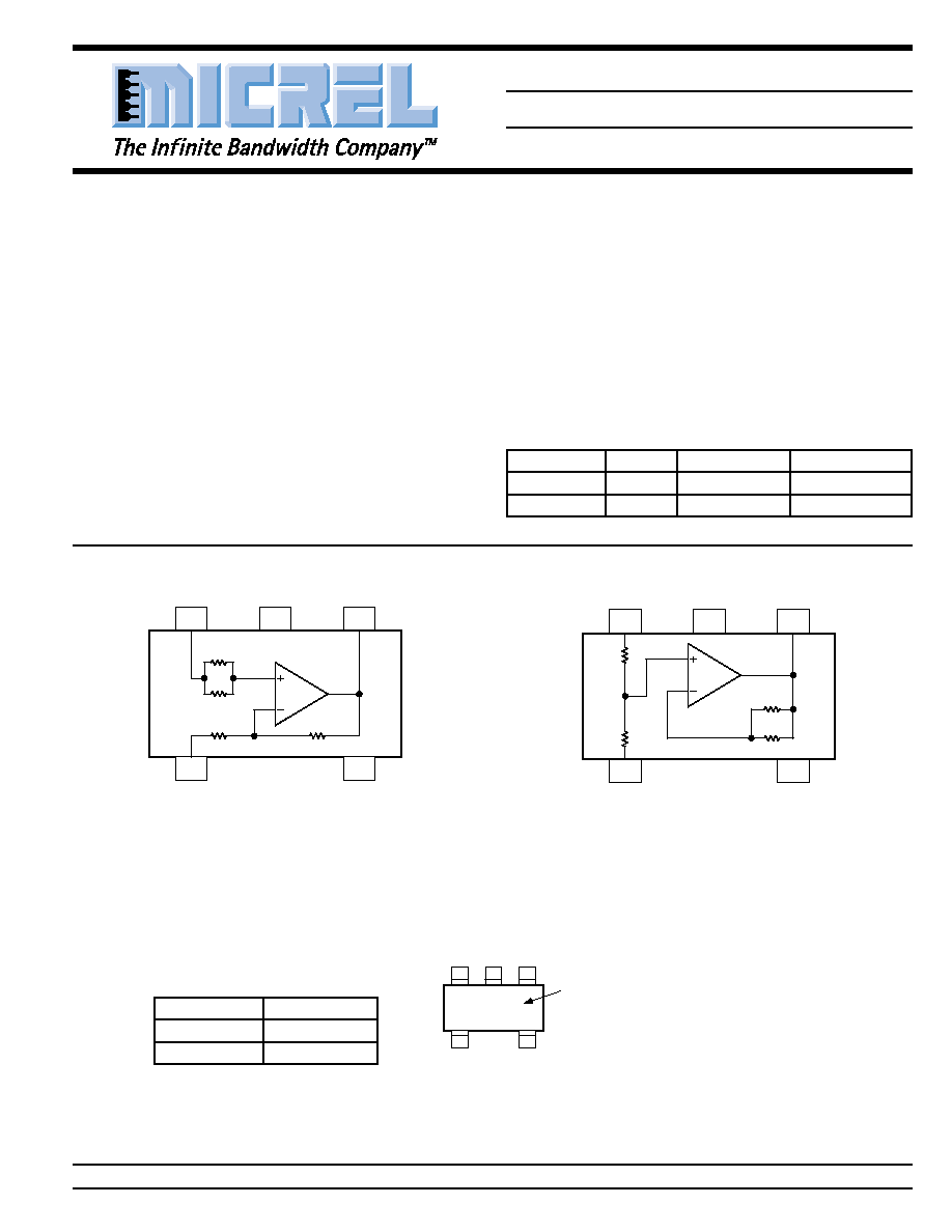
Functional Configuration
3
2
1
20k
20k
20k
4
5
IN+
V≠
OUT
IN≠
V+
20k
MIC6251
3
2
1
20k
20k
20k
4
5
IN+
V≠
OUT
IN≠
V+
20k
MIC6252
Pin Configuration
Part
Identification
OUT
V+
IN≠
IN+
Axx
1
3
4
5
2
V≠
SOT-23-5 (M5)
Part Number
Identification
MIC6251BM5
A51
MIC6252BM5
A52
IttyBitty and GainBlock are a trademarks of Micrel, Inc.
Micrel, Inc. ∑ 1849 Fortune Drive ∑ San Jose, CA 95131 ∑ USA ∑ tel + 1 (408) 944-0800 ∑ fax + 1 (408) 944-0970 ∑ http://www.micrel.com

MIC6251/6252
Micrel
MIC6251/6252
2
July 1998
Electrical Characteristics (Differential Supply)
V
V+
= +15V, V
V≠
= ≠15V; V
CM
= 0V, Note 1; T
A
= 25
∞
C, bold values indicate ≠40
∞
C
T
A
+85
∞
C, T
A
= T
J
; unless noted.
Symbol
Parameter
Condition
Min
Typ
Max
Units
G
E
Gain Error
MIC6251: A
V
= 2, V
O
=
±
10V
0.3
0.5
%
MIC6252: A
V
= 0.5, V
O
=
±
10V
0.3
0.5
%
G
NL
Gain Non-linearity
MIC6251: A
V
= 2, V
O
=
±
10V
0.01
%
MIC6252: A
V
= 0.5, V
O
=
±
10V
0.01
%
V
OS
Offset Voltage
MIC6251: Referred to output
4
14
mV
MIC6252: Referred to output
2
7
mV
TCV
OS
Average Offset Drift
7
µ
V/
∞
C
I
B
Input Bias Current
50
250
nA
V
CM
Input Voltage Range, Differential
Note 3
±
25
V
Input Volt. Range, Common Mode
±
13.5
±
13.8
V
CMRR
Common Mode Rejection Ratio
V
CM
= 27V, ≠13.5V to +13.5V
65
100
dB
PSRR
Power Supply Rejection Ratio
V
S
= 25V,
±
15V to
±
2.5V
65
110
dB
V
OUT
Maximum Output Voltage Swing
R
L
= 2k
±
12.5
±
14
V
B
W
Bandwidth
2
MHz
S
R
Slew Rate
6
V/
µ
s
I
S
Supply Current
1.3
2.0
mA
General Note : Devices are ESD protected; however, handling precautions are recommended.
Note 1:
IN+ and IN≠ pins on the MIC6252 are interchangeable.
Note 2:
Gain setting resistors are ratio-matched but have a
±
20% absolute tolerance
Note 3:
Limit input current to 1mA.
Note 4:
Human body model, 1.5k in series with 100pF.
Absolute Maximum Ratings
Supply Voltage (V
V+
≠ V
V≠
) ............................. 36V or
±
18V
Differential Input Voltage (V
IN+
≠ V
IN≠
) .......................
±
36V
Input Voltage (V
IN+
, V
IN≠
) ........................ V
V≠
≠ 0.3V to V
V+
Output Short Circuit Current Duration ...............................
Junction Temperature (T
J
) ........................................ 150
∞
C
Storage Temperature (T
S
) ....................... ≠65
∞
C to +150
∞
C
Lead Temperature (soldering, 10 sec.) ..................... 260
∞
C
ESD, Note 4 ............................................................... [TBD]
Operating Ratings
Supply Voltage .................................................... 4V to 32V
Ambient Temperature Range ..................... ≠40
∞
C to +85
∞
C
SOT-23-5 Thermal Resistance (
JA
) ..................... 325
∞
C/W
Pin Description
Pin Number
Pin Name
Pin Function
1
OUT
Amplifier Output
2
V≠
Negative Supply: Negative supply for split supply application or ground for
single supply application.
3
IN+
Noninverting Input: See "Electrical Characteristics: Note 1."
4
IN≠
Inverting Input: See "Electrical Characteristics: Note 1."
5
V+
Positive Supply