July 2003
1
MIC6315
MIC6315
Micrel
MIC6315
Open-Drain
µ
P Reset Circuit
General Description
The MIC6315 is an inexpensive reset generator circuit that
monitors power supplies in microprocessor based systems.
The function of this device is to assert a reset if either the
power supply drops below a designated reset threshold level
or /MR is forced low. Several different reset threshold levels
are available to accommodate 3V, 3.3V or 5V powered
systems.
The MIC6315 has an active low, open-drain /RESET output.
The reset output is guaranteed to remain asserted for a
minimum of either 20ms, 140ms, or 1100ms after V
CC
has
risen above the designed reset threshold level. The MIC6315
comes in a 4-pin SOT-143 package.
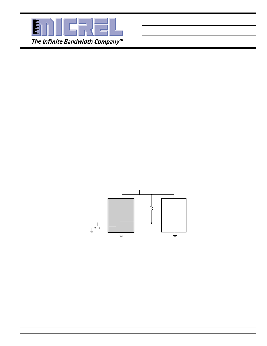
Typical Application
VCC
RESET
µP
RESET
VCC
MIC6315
VCC
MR
10k
Features
∑ Precision voltage monitor for 3V, 3.3V or 5V power
supplies
∑ /RESET remains valid with V
CC
as low as 1.4V
∑ <15
µ
A supply current
∑ 20ms, 40ms, or 1100ms minimum reset pulse widths
available
∑ Manual reset input
∑ 4-pin SOT-143 package
Applications
∑ Portable equipment
∑ Intelligent instruments
∑ Critical microprocessor power monitoring
∑ Printers/computers
∑ Embedded controllers
Micrel, Inc. ∑ 1849 Fortune Drive ∑ San Jose, CA 95131 ∑ USA ∑ tel + 1 (408) 944-0800 ∑ fax + 1 (408) 944-0970 ∑ http://www.micrel.com
MIC6315
Micrel
MIC6315
2
July 2003
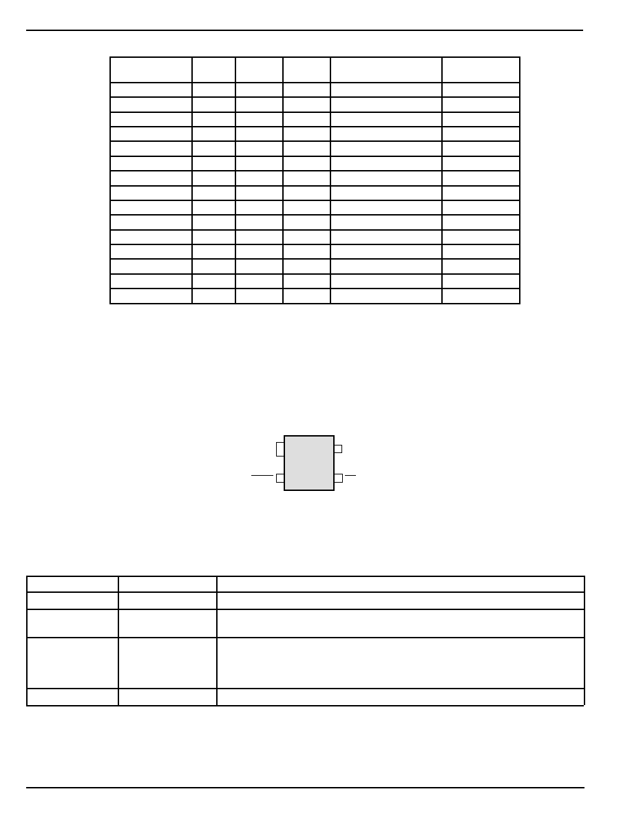
Pin Description
Pin Number
Pin Name
Pin Function
1
GND
IC Ground Pin.
2
/RESET
/RESET goes low if V
CC
falls below the reset threshold and remains asserted
for one reset timeout period after V
CC
exceeds the reset threshold.
3
/MR
Manual Reset Input. A logic low on /MR forces a reset. The reset will remain
asserted as long as /MR is held low and for one reset timeout period after /MR goes
high. This input can be shorted to ground via a switch or be driven by TTL or CMOS
logic. Float if unused.
4
VCC
Power Supply Input.
Pin Configuration
MR
1
2
4 V
CC
GND
MIC6315
RESET
3
MIC6315-xxDyU 4-Lead SOT-143
Ordering Information
(Note 1, 2)
Nominal
Min. t
RST
Part Number
Marking
V
TH
(V)
(ms)
Operating Temp. Range
Package
MIC6315-26D2U
NY
2.63
20
≠40
∞
C to +85
∞
C
4-lead SOT-143
MIC6315-29D2U
NM
2.93
20
≠40
∞
C to +85
∞
C
4-lead SOT-143
MIC6315-31D2U
zz
3.08
20
≠40
∞
C to +85
∞
C
4-lead SOT-143
MIC6315-44D2U
zz
4.38
20
≠40
∞
C to +85
∞
C
4-lead SOT-143
MIC6315-46D2U
zz
4.63
20
≠40
∞
C to +85
∞
C
4-lead SOT-143
MIC6315-26D3U
NR
2.63
140
≠40
∞
C to +85
∞
C
4-lead SOT-143
MIC6315-29D3U
NP
2.93
140
≠40
∞
C to +85
∞
C
4-lead SOT-143
MIC6315-31D3U
NU
3.08
140
≠40
∞
C to +85
∞
C
4-lead SOT-143
MIC6315-44D3U
zz
4.38
140
≠40
∞
C to +85
∞
C
4-lead SOT-143
MIC6315-46D3U
NX
4.63
140
≠40
∞
C to +85
∞
C
4-lead SOT-143
MIC6315-26D4U
NS
2.63
1100
≠40
∞
C to +85
∞
C
4-lead SOT-143
MIC6315-29D4U
NN
2.93
1100
≠40
∞
C to +85
∞
C
4-lead SOT-143
MIC6315-31D4U
zz
3.08
1100
≠40
∞
C to +85
∞
C
4-lead SOT-143
MIC6315-44D4U
zz
4.38
1100
≠40
∞
C to +85
∞
C
4-lead SOT-143
MIC6315-46D4U
NZ
4.63
1100
≠40
∞
C to +85
∞
C
4-lead SOT-143
Note 1.
All devices available in tape and reel only.
Note 2.
Parts not yet assigned an identification code are shown as "zz". Contact Micrel for details. Minimum
order may apply.

July 2003
3
MIC6315
MIC6315
Micrel
Electrical Characteristics
For typical values, V
CC
= 2.5V to 5.5V, T
A
= 25
∞
C; bold values indicate ≠40
∞
C
T
A
+85
∞
C; unless noted
Symbol
Parameter
Condition
Min
Typ
Max
Units
Operating Voltage Range
1.4
5.5
V
I
CC
Supply Current
V
CC
= 5.5V, no load
9
15
µ
A
V
CC
= 3.6V, no load
6
10
µ
A
V
TH
Reset Voltage Threshold
Note 4
V
TH
≠2.5%
V
TH
V
TH
+2.5%
V
t
RST
Reset Timeout Period
20
28
44
ms
140
200
320
ms
1100
1500
2500
ms
V
OL
/RESET Output Voltage
V
CC
> 4.25V, I
SINK
= 3.2mA
0.4
V
V
CC
> 2.5V, I
SINK
= 1.2mA
0.3
V
V
CC
> 1.4V, I
SINK
= 50
µ
A
0.3
V
/RESET Output Leakage
/RESET deasserted
1
µ
A
/MR Minimum Pulse Width
10
µ
s
/MR to Reset Delay
0.5
µ
s
V
IH
/MR Input Threshold
V
TH
> 4.0V
2.3
V
V
TH
> 4.0V
0.7
◊◊
◊◊
◊
V
CC
V
V
IL
/MR Input Threshold
V
TH
> 4.0V
0.8
V
V
TH
> 4.0V
0.25
◊◊
◊◊
◊
V
CC
V
/MR Pull-Up Resistance
10
20
30
k
/MR Glitch Immunity
100
ns
Note 1.
Exceeding the absolute maximum rating may damage the device.
Note 2.
The device is not guaranteed to function outside its operating rating.
Note 3.
Devices are ESD sensitive. Handling precautions recommended. Human body model, 1.5k in series with 100pF.
Note 4.
Various reset thresholds available. See ordering information or contact factory.
Absolute Maximum Ratings
(Note 1)
Terminal Voltage
(V
CC
, /RESET) ...................................... ≠0.3V to 6.0V
(/MR) ........................................ ≠0.3V to (V
CC
+ 0.3V)
Rate of Rise (V
CC
) ................................................. 100V/
µ
s
Input Current (V
CC
, /MR) ............................................ 20mA
Output Current (/RESET) ........................................... 20mA
Lead Temperature (soldering, 10 sec.) ..................... 300
∞
C
Storage Temperature (T
S
) ........................ ≠65
∞
C to 150
∞
C
ESD Rating, Note 3
Operating Ratings
(Note 2)
Operating Temperature Range .................. ≠40
∞
C to +85
∞
C
Input Voltage (/RESET) .................................... GND ≠ 5.5V
Power Dissipation (T
A
= +70
∞
C) .............................. 320mW
MIC6315
Micrel
MIC6315
4
July 2003
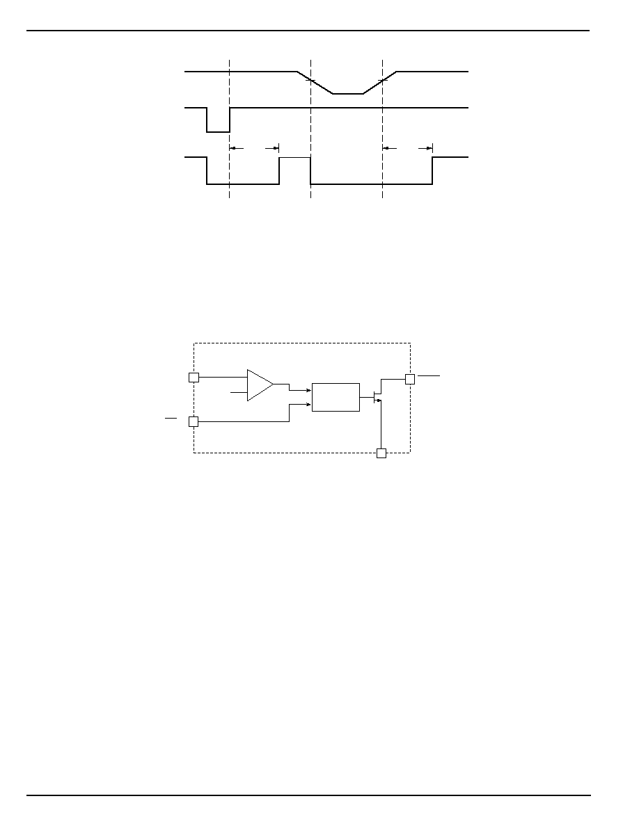
Functional Diagram
+
-
Reset
Threshold (V)
VCC (4)
RESET (2)
GND (1)
RESET
GENERATOR
MR (3)
Timing Diagram
V
CC
/MR
/RESET
t
RST
t
RST
V
TH
Reset Timing Diagram
July 2003
5
MIC6315
MIC6315
Micrel
Applications Information
Microprocessor Reset
The /RESET pin is asserted whenever V
CC
falls below the
reset threshold voltage or if /MR (manual reset) is forced low.
The /RESET pin remains asserted for the duration of the reset
timeout period after V
CC
has risen above the reset threshold
or /MR has returned high. The reset function ensures the
microprocessor is properly reset and powers up in a known
condition after a power failure. /RESET will remain valid with
V
CC
as low as 1.4V.
The /RESET output is a simple open-drain N-channel MOS-
FET structure. A pull-up resistor must be used to pull this
output up to some voltage. For most applications, this voltage
will be the same power supply that supplies V
CC
to the
MIC6315. It is possible however to tie this resistor to some
other voltage. This will allow the MIC6315 to monitor one
voltage while level-shifting the /RESET output to some other
voltage. The pull-up voltage must be limited to 6.0V or less
(absolute maximum) to avoid damage to the MIC6315. The
resistor must be small enough to supply current to the inputs
and leakage paths that are driven by the /RESET output.
/RESET Valid at Low Voltage
As V
CC
drops to 0V, the MIC6315 will no longer be able to pull
the /RESET output low. At this point, the pull-up resistor will
pull the output high. The value of the pull-up resistor and the
voltage it is connected to will affect the point at which this
happens.
Wire OR'ing The /RESET Output
Because the RESET output is open-drain, several reset
sources can be wire-ORed in parallel to allow resets from
multiple sources.
V
CC
Transients
The MIC6315 is relatively immune to negative-going V
CC
glitches below the reset threshold. Typically, a negative-
going transient 125mV below the reset threshold with a
duration of 25
µ
s or less will not cause an unwanted reset. If
additional transient immunity is needed, a bypass capacitor
can be placed a close as possible to the MIC6315.
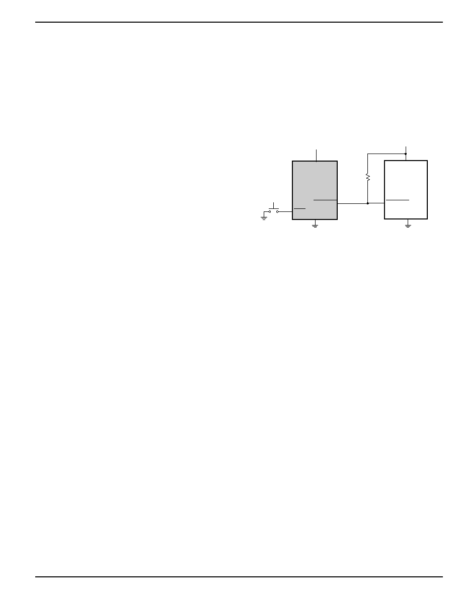
VCC
RESET
5V SYSTEM
RESET
VCC
MIC6315
+5.0V
MR
10k
+3.3V
MIC6315 Used in a Multiple Supply System