MIC68200
2A Sequencing LDO with Tracking
and Ramp ControlTM
MLF and
Micro
LeadFrame are trademarks of Amkor Technology, Inc.
Micrel Inc. ∑ 2180 Fortune Drive ∑ San Jose, CA 95131 ∑ USA ∑ tel +1 (408) 944-0800 ∑ fax + 1 (408) 474-1000 ∑ http://www.micrel.com
December 2005
M9999-121905
(408) 955-1690
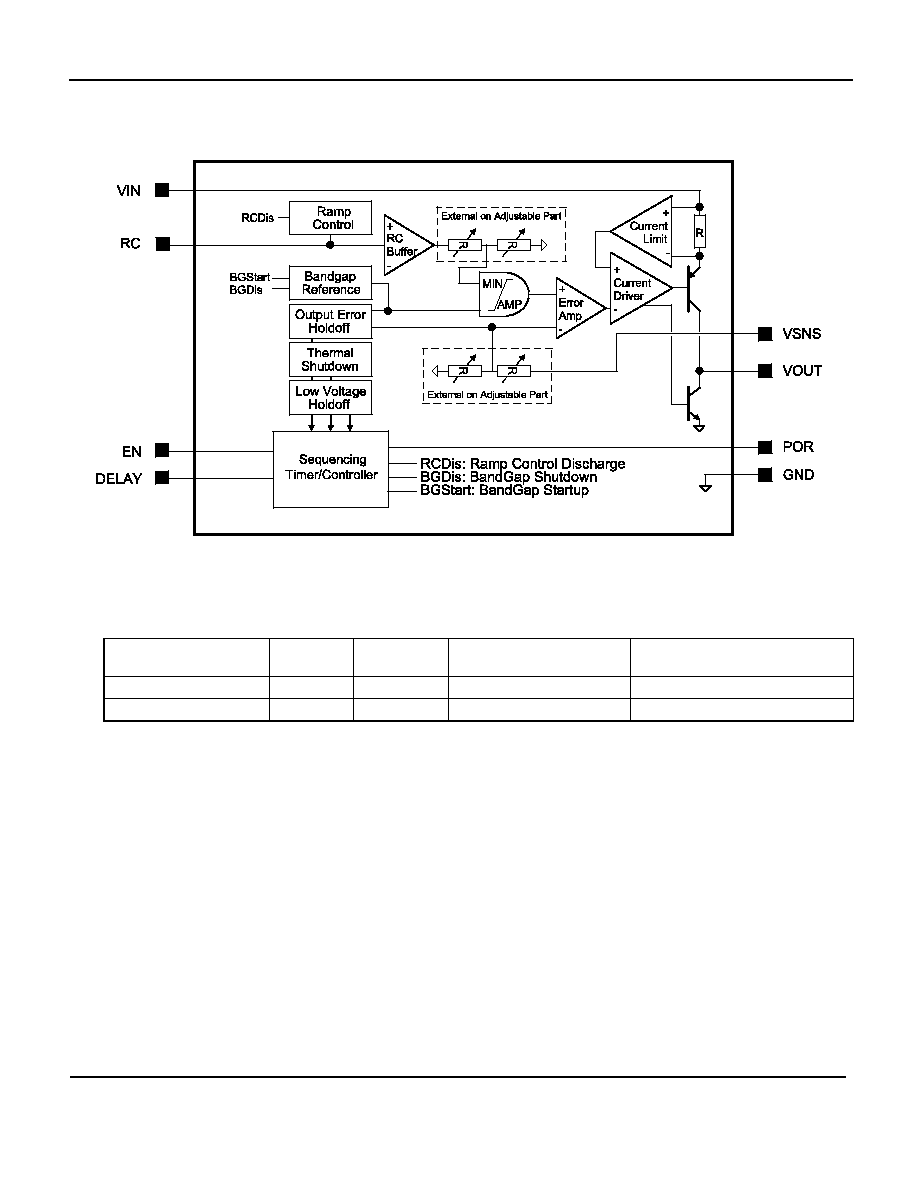
General Description
The MIC68200 is a high peak current LDO regulator
designed specifically for powering applications such
as FPGA core voltages that require high start up
current with lower nominal operating current. Capable
of sourcing 2A of current for start-up, the MIC68200
provides high power from a small MLFTM leadless
package. The MIC68200 can also implement a variety
of power-up and power-down protocols such as
sequencing, tracking, and ratiometric tracking.
The MIC68200 operates from a wide input range of
1.65V to 5.5V, which includes all of the main supply
voltages commonly available today. It is designed to
drive digital circuits requiring low voltage at high
currents (i.e. PLDs, DSP, microcontroller, etc.). The
MIC68200 incorporates a delay pin (Delay) for control
of power on reset output (POR) at turn-on and power-
down delay at turn-off. In addition, there is a ramp
control pin (RC) for either tracking applications or
output voltage slew rate adjustment at turn-on and
turn-off. This is important in applications where the
load is highly capacitive and in-rush currents can
cause supply voltages to fail and microprocessors or
other complex logic chips to hang up.
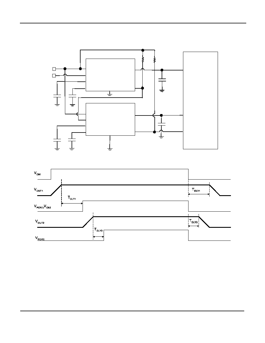
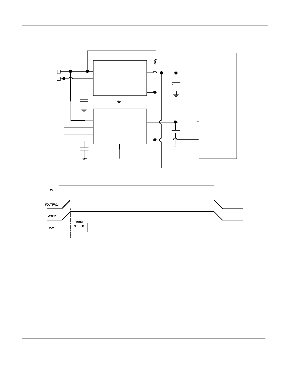
Multiple MIC68200s can be daisy chained in two
modes. In tracking mode the output voltage of the
Master drives the RC pin of a Slave so that the Slave
tracks the main regulator during turn-on and turn-off.
In sequencing mode the POR of the Master drives the
enable (EN) of the Slave so that it turns on after the
Master and turns off before (or after) the Master. This
behavior is critical for power-up and power-down
control in multi-output power supplies. The MIC68200
is fully protected offering both thermal and current limit
protection and reverse current protection.
The MIC68200 has a junction temperature range of
≠40∞C to +125∞C and is available in fixed as well as
an adjustable option. There is also an adjustable
option. The MIC68200 is offered in the tiny 10-pin
3mm x 3mm MLFTM package.
Features
∑ Stable with 4.7uF ceramic capacitor
∑ Input voltage range: 1.65V to 5.5V
∑ +1.0% initial output tolerance
∑ 2A maximum output current ≠ peak start up
∑ 1A Continuous Operating Current
∑
Tracking on turn-on and turn-off with pin
strapping
∑
Timing Controlled Sequencing On/Off
∑
Programmable Ramp ControlTM for in-rush
current limiting and slew rate control of the
output voltage
∑ Power-on Reset (POR) supervisor with
programmable delay time
∑
Single Master can control multiple Slave
regulators with tracking output voltages
∑
Tiny 3mm x 3mm MLF
TM
package
∑ Maximum dropout (V
IN
≠ V
OUT
) of 500mV over
temperature at 1A output current
∑ Fixed and Adjustable Output Voltages
∑ Excellent line and load regulation specifications
∑ Logic controlled shutdown
∑ Thermal shutdown and current limit protection
Applications
∑ FPGA/PLD Power Supply
∑ Networking/Telecom
Equipment
∑ Microprocessor Core Voltage
∑ High Efficiency Linear Post Regulator
∑ Sequenced or Tracked Power Supply
Micrel, Inc.
MIC68200
December 2005
5
M9999-121905
(408) 955-1690
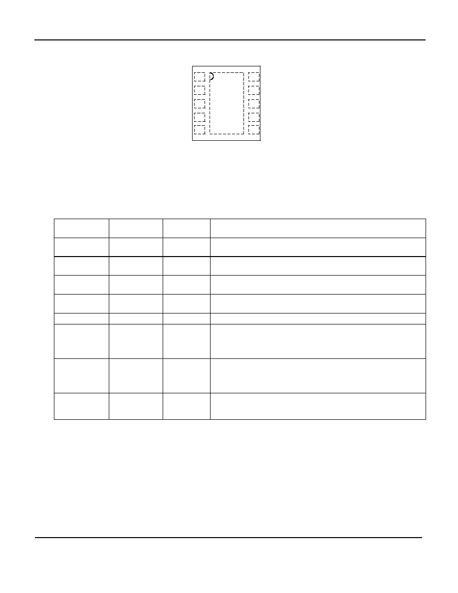
Pin Configuration
EP
5
1
1
9
8
7
2
3
4
0
6
10-Pin 3mm ◊ 3mm MLF (ML)
MIC68200-x.xYML (Fixed)
MIC68200YML (Adjustable)
Pin Description
(Pin Numbering may change depending upon layout considerations)
3x3 MLF-10
Fixed
3x3 MLF-10
Adjustable
Pin Name
Pin Function
1,2 1,2
VIN
Input: Input voltage supply pin. Place a capacitor to ground to
bypass the input supply
3 3
Delay
Delay: Capacitor to ground sets internal delay timer. Timer delays
power-on reset (POR) output at turn-on and ramp down at turn-off.
4 4
RC
Ramp Control: Voltage driven for tracking applications. Capacitor to
ground sets slew rate during start-up.
5 5
EN
Enable (Input): CMOS compatible input. Logic high = enable and
logic low = shutdown.
6, EP
6, EP
GND
Ground: EP is connected to ground on 3x3 MLF-10L.
7 7
POR
Power-on Reset: Open-drain output device indicates when the
output is in regulation. High (open) means device is regulating within
10%. POR onset can be delayed using a single capacitor from
Delay-to-ground.
8
8
ADJ / SNS
Adjustable regulators: Feedback input. Connect to external resistor
voltage divider.
Fixed regulators: Sense pin. Connect to output at load for point-of-
load regulation.
9, 10
9,10
VOUT
Output Voltage: Output of voltage regulator. Place capacitor to
ground to bypass the output voltage. Minimum load current is 100uA.
Nominal bypass capacitor is 4.7uf ceramic.