June 1998
1
MIC7111
MIC7111
Micrel
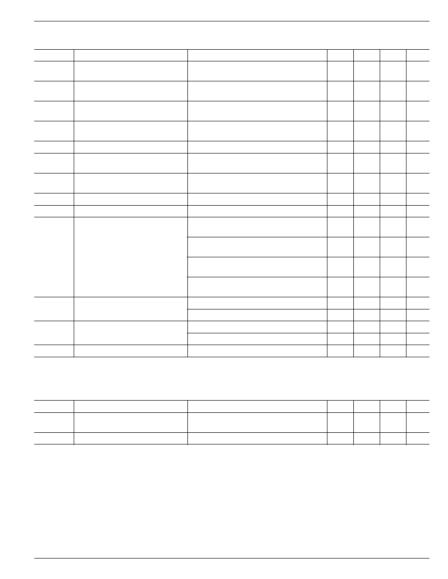
Pin Description
Pin Number
Pin Name
Pin Function
1
OUT
Amplifier Output
2
V+
Positive Supply
3
IN+
Noninverting Input
4
IN≠
Inverting Input
5
V≠
Negative Suppy
MIC7111
1.8V IttyBittyTM Rail-to-Rail Input/Output Op Amp
Preliminary Information
Functional Configuration
OUT
V+
IN≠
IN+
1
3
4
5
2
V≠
SOT-23-5 (M5)
Pin Configuration
OUT
V+
IN≠
IN+
1
3
4
5
2
V≠
A13
Part
Identification
Micrel, Inc. ∑ 1849 Fortune Drive ∑ San Jose, CA 95131 ∑ USA ∑ tel + 1 (408) 944-0800 ∑ fax + 1 (408) 944-0970 ∑ http://www.micrel.com
Features
∑ Small footprint SOT-23-5 package
∑ Guaranteed performance at 1.8V, 2.7V, 5V, and 10V
∑ 15
µ
A typical supply current at 1.8V
∑ 25kHz gain-bandwidth at 5V
∑ Output swing to within 1mV of rails
with 1.8V supply and 100k
load
∑ Suitable for driving capacitive loads
Applications
∑ Wireless and cellular communications
∑ GaAs RF amplifier bias amplifier
∑ Current sensing for battery chargers
∑ Reference voltage buffer
∑ Transducer linearization and interface
∑ Portable computing
Ordering Information
Part Number
Junction Temp. Range
Package
MIC7111BM5
≠40
∞
C to +85
∞
C
SOT-23-5
General Description
The MIC7111 is a micropower operational amplifier featuring
rail-to-rail input and output performance in Micrel's IttyBitty
TM
SOT-23-5 package. The MIC7111 is ideal for systems where
small size is a critical consideration.
The MIC7111 is designed to operate from 1.8V to 11V power
supplies.
The MIC7111 benefits small battery operated portable elec-
tronic devices where small size and the ability to place the
amplifier close to the signal source are primary design
concerns.
For other package options, please contact the factory.
IttyBitty is a trademark of Micrel, Inc.

MIC7111
Micrel
MIC7111
2
June 1998
Absolute Maximum Ratings
(Note 1)
Supply Voltage (V
V+
≠ V
V≠
) ........................................... 12V
Differential Input Voltage (V
IN+
≠ V
IN≠
) ...........
±
(V
V+
≠ V
V≠
)
I/O Pin Voltage (V
IN
, V
OUT
), Note 2
............................................. V
V+
+ 0.3V to V
V≠
≠ 0.3V
Junction Temperature (T
J
) ...................................... +150
∞
C
Storage Temperature ............................... ≠65
∞
C to +150
∞
C
Lead Temperature (soldering, 10 sec.) ..................... 260
∞
C
ESD, Note 5 .................................................................. 2kV
Operating Ratings
(Note 1)
Supply Voltage (V
V+
≠ V
V≠
) .............................. 1.8V to 11V
Junction Temperature (T
J
) ......................... ≠40
∞
C to +85
∞
C
Max. Junction Temperature (T
J(max)
), Note 3 ........... +85
∞
C
Package Thermal Resistance (
JA
), Note 4.......... 325
∞
C/W
Max. Power Dissipation ............................................ Note 3
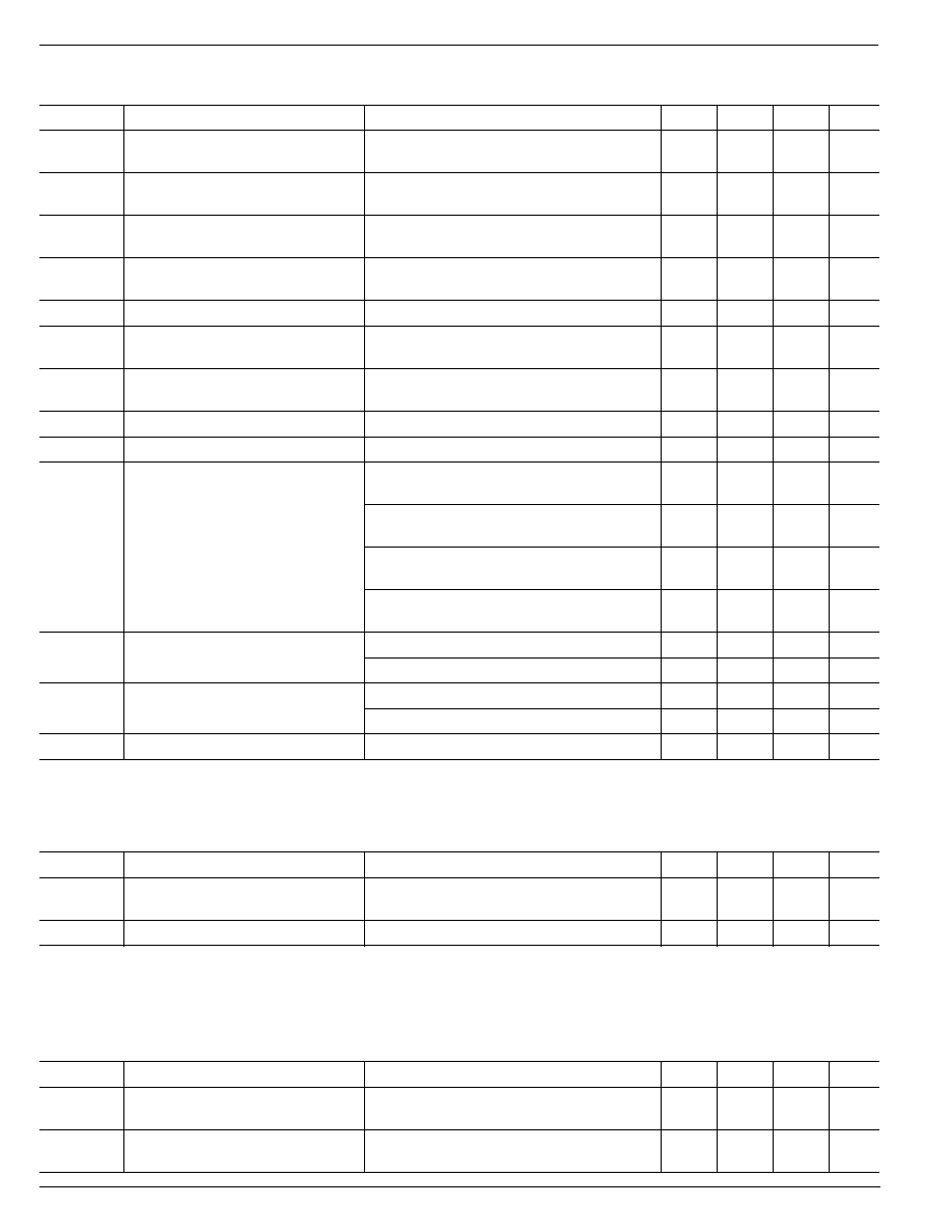
DC Electrical Characteristics (1.8V)
V
V+
= +1.8V, V
V≠
= 0V, V
CM
= V
OUT
= V
V+
/2; R
L
= 1M; T
J
= 25
∞
C, bold values indicate ≠40
∞
C
T
J
+85
∞
C; unless noted
Symbol
Parameter
Condition
Min
Typ
Max
Units
V
OS
Input Offset Voltage
0.9
7
mV
9
mV
TCV
OS
Input Offset Voltage
2.0
µ
V/
∞
C
Temperature Drift
I
B
Input Bias Current
1
10
pA
500
pA
I
OS
Input Offset Current
0.01
0.5
pA
75
pA
R
IN
Input Resistance
>10
T
+PSRR
Positive Power Supply
1.8V
V
V+
5V, V
V≠
= 0V,
60
85
dB
Rejection Ratio
V
CM
= V
OUT
= 0.9V
≠PSRR
Negative Power Supply
≠1.8V
V
V≠
≠5V, V
V+
= 0V,
60
85
dB
Rejection Ratio
V
CM
= V
OUT
= ≠0.9V
CMRR
Common-Mode Rejection Ratio
V
CM
= ≠0.2V to +2.0V
50
70
dB
C
IN
Common Mode Input Capacitance
3
pF
V
OUT
Output Voltage Swing
output high, R
L
= 100k,
0.14
1
mV
specified as V
V+
≠ V
OUT
1
mV
output low, R
L
= 100k
0.14
1
mV
1
mV
output high, R
L
= 2k,
6.8
23
mV
specified as V
V+
≠ V
OUT
34
mV
output low, R
L
= 2k
6.8
23
mV
34
mV
I
SC
Output Short Circuit Current
sourcing, V
OUT
= 0V
15
25
mA
Note 6
sinking, V
OUT
= 1.8V
15
25
mA
A
VOL
Voltage Gain
sourcing
400
V/mV
sinking
400
V/mV
I
s
Supply Current
V
V+
= 1.8V, V
OUT
= V
V+
/2
15
35
µ
A
AC Electrical Characteristics (1.8V)
V+ = +1.8V, V≠ = 0V, V
CM
= V
OUT
= V
V+
/2; R
L
= 1M; T
J
= 25
∞
C, bold values indicate ≠40
∞
C
T
J
+85
∞
C; unless noted
SR
Slew Rate
voltage follower, 1V step, R
L
= 100k@0.9V
0.015
V/
µ
s
V
OUT
= 1V
P≠P
GBW
Gain Bandwidth Product
25
kHz
June 1998
3
MIC7111
MIC7111
Micrel
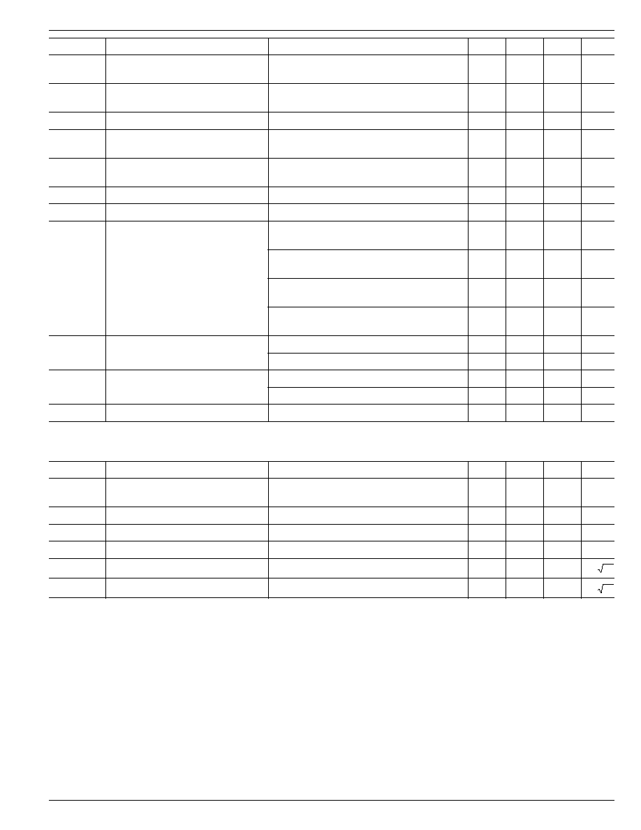
DC Electrical Characteristics (2.7V)
V
V+
= +2.7V, V
V≠
= 0V, V
CM
= V
OUT
= V
V+
/2; R
L
= 1M; T
J
= 25
∞
C, bold values indicate ≠40
∞
C
T
J
+85
∞
C; unless noted
Symbol
Parameter
Condition
Min
Typ
Max
Units
V
OS
Input Offset Voltage
0.9
7
mV
9
mV
TCV
OS
Input Offset Voltage
2.0
µ
V/
∞
C
Temperature Drift
I
B
Input Bias Current
1
10
pA
500
pA
I
OS
Input Offset Current
0.01
0.5
pA
75
pA
R
IN
Input Resistance
>10
T
+PSRR
Positive Power Supply
2.7V
V
V+
5V, V
V≠
= 0V,
60
90
dB
Rejection Ratio
V
CM
= V
OUT
= 1.35V
≠PSRR
Negative Power Supply
≠2.7V
V
V≠
≠5V, V
V+
= 0V,
60
90
dB
Rejection Ratio
V
CM
= V
OUT
= ≠1.35V
CMRR
Common-Mode Rejection Ratio
V
CM
= ≠0.2V to +2.9V
52
75
dB
C
IN
Common Mode Input Capacitance
3
pF
V
OUT
Output Voltage Swing
output high, R
L
= 100k,
0.2
1
mV
specified as V
V+
≠ V
OUT
1
mV
output low, R
L
= 100k
0.2
1
mV
1
mV
output high, R
L
= 2k,
10
33
mV
specified as V
V+
≠ V
OUT
50
mV
output low, R
L
= 2k
10
33
mV
50
mV
I
SC
Output Short Circuit Current
sourcing, V
OUT
= 0V
30
50
mA
Note 6
sinking, V
OUT
= 2.7V
30
50
mA
A
VOL
Voltage Gain
sourcing
400
V/mV
sinking
400
V/mV
I
s
Supply Current
V
V+
= 2.7V, V
OUT
= V
V+
/2
17
42
µ
A
AC Electrical Characteristics (2.7V)
V+ = +2.7V, V≠ = 0V, V
CM
= V
OUT
= V
V+
/2; R
L
= 1M; T
J
= 25
∞
C, bold values indicate ≠40
∞
C
T
J
+85
∞
C; unless noted
Symbol
Parameter
Condition
Min
Typ
Max
Units
SR
Slew Rate
voltage follower, 1V step, R
L
= 100k@1.35V
0.015
V/
µ
s
V
OUT
= 1V
P≠P
GBW
Gain Bandwidth Product
25
kHz
MIC7111
Micrel
MIC7111
4
June 1998
DC Electrical Characteristics (5V)
V
V+
= +5.0V, V
V≠
= 0V, V
CM
= V
OUT
= V
V+
/2; R
L
= 1M; T
J
= 25
∞
C, bold values indicate ≠40
∞
C
T
J
+85
∞
C; unless noted
Symbol
Parameter
Condition
Min
Typ
Max
Units
V
OS
Input Offset Voltage
0.9
7
mV
9
mV
TCV
OS
Input Offset Voltage
2.0
µ
V/
∞
C
Temperature Drift
I
B
Input Bias Current
1
10
pA
500
pA
I
OS
Input Offset Current
0.01
0.5
pA
75
pA
R
IN
Input Resistance
>10
T
+PSRR
Positive Power Supply
5V
V
V+
10V, V
V≠
= 0V,
65
95
dB
Rejection Ratio
V
CM
= V
OUT
= 2.5V
≠PSRR
Negative Power Supply
≠5V
V
V≠
≠10V, V
V+
= 0V,
65
95
dB
Rejection Ratio
V
CM
= V
OUT
= ≠2.5V
CMRR
Common-Mode Rejection Ratio
V
CM
= ≠0.2V to +5.2V
57
80
dB
C
IN
Common Mode Input Capacitance
3
pF
V
OUT
Output Voltage Swing
output high, R
L
= 100k,
0.3
1.5
mV
specified as V
V+
≠ V
OUT
1.5
mV
output low, R
L
= 100k
0.3
1.5
mV
1.5
mV
output high, R
L
= 2k,
15
50
mV
specified as V
V+
≠ V
OUT
75
mV
output low, R
L
= 2k
15
50
mV
75
mV
I
SC
Output Short Circuit Current
sourcing, V
OUT
= 0V
80
100
mA
Note 6
sinking, V
OUT
= 5V
80
100
mA
A
VOL
Voltage Gain
sourcing
500
V/mV
sinking
500
V/mV
I
S
Supply Current
V
V+
= 5V, V
OUT
= V
V+
/2
20
50
µ
A
AC Electrical Characteristics (5V)
V+ = +5V, V≠ = 0V, V
CM
= V
OUT
= V
V+
/2; R
L
= 1M; T
J
= 25
∞
C, bold values indicate ≠40
∞
C
T
J
+85
∞
C; unless noted
Symbol
Parameter
Condition
Min
Typ
Max
Units
SR
Slew Rate
voltage follower, 1V step, R
L
= 100k@1.5V
0.02
V/
µ
s
V
OUT
= 1V
P≠P
GBW
Gain Bandwidth Product
25
kHz
DC Electrical Characteristics (10V)
V
V+
= +10V, V
V≠
= 0V, V
CM
= V
OUT
= V
V+
/2; R
L
= 1M; T
J
= 25
∞
C, bold values indicate ≠40
∞
C
T
J
+85
∞
C; unless noted
Symbol
Parameter
Condition
Min
Typ
Max
Units
V
OS
Input Offset Voltage
0.9
7
mV
9
mV
TCV
OS
Input Offset Voltage
2.0
µ
V/
∞
C
Temperature Drift
June 1998
5
MIC7111
MIC7111
Micrel
Symbol
Parameter
Condition
Min
Typ
Max
Units
I
B
Input Bias Current
1
10
pA
500
pA
I
OS
Input Offset Current
0.01
0.5
pA
75
pA
R
IN
Input Resistance
>10
T
+PSRR
Positive Power Supply
5V
V
V+
10V, V
V≠
= 0V,
65
95
dB
Rejection Ratio
V
CM
= V
OUT
= 2.5V
≠PSRR
Negative Power Supply
≠5V
V
V≠
≠10V, V
V+
= 0V,
65
95
dB
Rejection Ratio
V
CM
= V
OUT
= ≠2.5V
CMRR
Common-Mode Rejection Ratio
V
CM
= ≠0.2V to +10.2V
60
85
dB
C
IN
Common Mode Input Capacitance
3
pF
V
OUT
Output Voltage Swing
output high, R
L
= 100k,
0.45
2.5
mV
specified as V
V+
≠ V
OUT
2.5
mV
output low, R
L
= 100k
0.45
2.5
mV
2.5
mV
output high, R
L
= 2k,
24
80
mV
specified as V
V+
≠ V
OUT
120
mV
output low, R
L
= 2k
24
80
mV
120
mV
I
SC
Output Short Circuit Current
sourcing, V
OUT
= 0V
100
200
mA
Note 6
sinking, V
OUT
= 10V
100
200
mA
A
VOL
Voltage Gain
sourcing
500
V/mV
sinking
500
V/mV
I
S
Supply Current
V
V+
= 10V, V
OUT
= V
V+
/2
25
65
µ
A
AC Electrical Characteristics (10V)
V+ = +10V, V≠ = 0V, V
CM
= V
OUT
= V
V+
/2; R
L
= 1M; T
J
= 25
∞
C, bold values indicate ≠40
∞
C
T
J
+85
∞
C; unless noted
Symbol
Parameter
Condition
Min
Typ
Max
Units
SR
Slew Rate
voltage follower, 1V step, R
L
= 100k@1.35V
0.02
V/
µ
s
V
OUT
= 1V
P≠P
GBW
Gain Bandwidth Product
25
kHz
M
Phase Margin
50
∞
G
M
Gain Margin
15
dB
e
N
Input Referred Voltage Noise
f = 1kHz, V
CM
= 1.0V
110
nV/ Hz
i
N
Input Referred Current Noise
f = 1kHz
0.03
pA/ Hz
General Notes: Devices are ESD protected; however, handling precautions are recommended. All limits guaranteed by testing on statistical analysis.
Note 1:
Absolute maximum ratings indicate limits beyond which damage to the component may occur. Electrical specifications do not apply when
operating the device outside its recommended operating ratings.
Note 2:
I/O Pin Voltage is any external voltage to which an input or output is referenced.
Note 3:
The maximum allowable power dissipation is a function of the maximum junction temperature, T
J(max)
; the junction-to-ambient thermal
resistance,
JA
; and the ambient temperature, T
A
. The maximum allowable power dissipation at any ambient temperature is calculated using:
P
D
= (T
J(max)
≠ T
A
)
˜
JA
. Exceeding the maximum allowable power dissipation will result in excessive die temperature.
Note 4:
Thermal resistance,
JA
, applies to a part soldered on a printed-circuit board.
Note 5:
Human body model, 1.5k in series with 100pF.
Note 6:
Short circuit may cause the device to exceed maxium allowable power dissipation. See Note 3.