
March 1999
1
MIC7122
MIC7122
Micrel
MIC7122
Micrel
MIC7122
Rail-to-Rail Dual Op Amp
Preliminary Information
General Description
The MIC7122 is a dual high-performance CMOS operational
amplifier featuring rail-to-rail inputs and outputs.
The input common-mode range extends beyond the rails by
300mV, and the output voltage swings to within 150
µ
V of both
rails when driving a 100k
load.
The amplifiers operate from 2.2V to 15V and are fully speci-
fied at 2.2V, 5V, and 15V. Gain bandwidth and slew rate are
750kHz and 0.7V/
µ
s, respectively at 2.2V supply.
The MIC7122 is available in the MM8TM 8-lead MSOP pack-
age.
Features
∑ Small footprint MSOP-8 package
∑ 350
µ
A supply current per op amp at 2.2V supply
∑ Guaranteed 2.2V, 5V, and 15V performance
∑ 750kHz gain-bandwidth product at 2.2V supply
∑ 0.01% total harmonic distortion at 1kHz (15V, 2k
)
∑ Drives 200pF at 5V and greater supply voltages
Applications
∑ Battery-powered instrumentation
∑ PCMCIA, USB peripherals
∑ Portable computers and PDAs
Ordering Information
Part Number
Temperature Range
Package
MIC7122BMM
≠40
∞
C to +85
∞
C
MSOP-8
Micrel, Inc. ∑ 1849 Fortune Drive ∑ San Jose, CA 95131 ∑ USA ∑ tel + 1 (408) 944-0800 ∑ fax + 1 (408) 944-0970 ∑ http://www.micrel.com
MM8 is a trademark of Micrel, Inc.
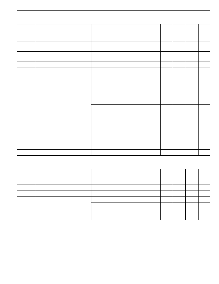
Pin Description
Pin Number
Pin Name
Pin Function
1 / 7
OUTA / OUTB
Amplifier Outputs
2 / 6
INA≠ / INB≠
Inverting Inputs
3 / 5
INA+ / INB+
Noninverting Inputs
4
V≠
Negative Supply: Negative supply for split supply application or ground for
single supply applications.
8
V+
Positive Supply
Pin Configuration
1
2
3
4
8
7
6
5
V+
OUT B
INB≠
INB+
OUT A
IN A≠
IN A+
V≠
MSOP-8 (MM)
1
2
3
4
8
7
6
5
A
B

MIC7122
Micrel
MIC7122
2
March 1999
Absolute Maximum Ratings
(Note 1)
Supply Voltage (V
V+
≠ V
V≠
) ........................................ 16.5V
Differential Input Voltage (V
IN+
≠ V
IN≠
) .......................
±
10V
I/O Pin Voltage (V
IN
, V
OUT
), Note 3
............................................. V
V+
+ 0.3V to V
V≠
≠ 0.3V
Junction Temperature (T
J
) ...................................... +150
∞
C
Storage Temperature ............................... ≠65
∞
C to +150
∞
C
Lead Temperature (soldering, 10 sec.) ..................... 260
∞
C
ESD, Note 6 .............................................................. 1000V
Operating Ratings
(Note 2)
Supply Voltage (V
V+
≠ V
V≠
) .............................. 2.2V to 15V
Junction Temperature (T
J
) ......................... ≠40
∞
C to +85
∞
C
Max. Junction Temperature (T
J(max)
), Note 4 ......... +125
∞
C
Max. Power Dissipation ............................................ Note 4
Package Thermal Resistance, Note 5
MSOP-8 (
JA
) .................................................... 200
∞
C/W
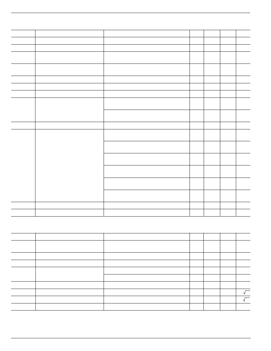
DC Electrical Characteristics (2.2V)
V
V+
= +2.2V, V
V≠
= 0V, V
CM
= V
OUT
= V
V+
/2; R
L
= 1M
; T
J
= 25
∞
C, bold values indicate ≠40
∞
C
T
J
+85
∞
C; Note 7; unless noted
Symbol
Parameter
Condition
Min
Typ
Max
Units
V
OS
Input Offset Voltage
0.5
9
mV
TCV
OS
Input Offset Voltage Average Drift
3.0
µ
V/
∞
C
I
B
Input Bias Current
1.0
10
pA
64
500
pA
I
OS
Input Offset Current
0.5
5
pA
32
250
pA
R
IN
Input Resistance
>1
T
CMRR
Common-Mode Rejection Ratio
-0.3V
V
CM
2.5V, Note 9
45
65
dB
±
PSRR
Power Supply Rejection Ratio
V
V+
=
V
V≠
= 1.1V to 2.5V, V
OUT
= V
CM
= 0
60
85
dB
C
IN
Common-Mode Input Capacitance
3
pF
V
O
Output Swing
output high, R
L
= 100k,
0.15
1
mV
specified as V
V+
≠ V
OUT
1
mV
output low, R
L
= 100k
0.15
1
mV
1
mV
output high, R
L
= 2k
8
33
mV
specified as V
V+
≠ V
OUT
50
mV
output low, R
L
= 2k
8
33
mV
50
mV
output high, R
L
= 600
26
110
mV
specified as V
V+
≠ V
OUT
165
mV
output low, R
L
= 600
26
110
mV
165
mV
I
SC
Output Short Circuit Current
sinking or sourcing, Note 8
20
50
mA
I
S
Supply Current
both amplifiers
0.7
1.6
mA
AC Electrical Characteristics (2.2V)
V
V+
= 2.2V, V
V≠
= 0V, V
CM
= V
OUT
= V
V+
/2; R
L
= 1M
; T
J
= 25
∞
C, bold values indicate ≠40
∞
C
T
J
+85
∞
C; Note 7; unless noted
Symbol
Parameter
Condition
Min
Typ
Max
Units
SR
Slew Rate
0.7
V/
µ
s
GBW
Gain-Bandwidth Product
750
kHz
m
Phase Margin
C
L
= 0pF
80
∞
C
L
= 200pF
40
∞
G
m
Gain Margin
10
dB
Interamplifier Isolation
Note 12
90
dB
March 1999
3
MIC7122
MIC7122
Micrel
DC Electrical Characteristics (5V)
V
V+
= +5.0V, V
V≠
= 0V, V
CM
= 1.5V, V
OUT
= V
V+
/2; R
L
= 1M
; T
J
= 25
∞
C, bold values indicate ≠40
∞
C
T
J
+85
∞
C; Note 7; unless noted
Symbol
Parameter
Condition
Min
Typ
Max
Units
V
OS
Input Offset Voltage
0.5
9
mV
TCV
OS
Input Offset Voltage Average Drift
3.0
µ
V/
∞
C
I
B
Input Bias Current
1.0
10
pA
64
500
pA
I
OS
Input Offset Current
0.5
5
pA
32
250
pA
R
IN
Input Resistance
>1
T
CMRR
Common-Mode Rejection Ratio
-0.3V
V
CM
5.3V, Note 9
55
75
dB
±
PSRR
Power Supply Rejection Ratio
V
V+
=
V
V≠
= 2.5V to 7.5V, V
OUT
= V
CM
= 0
55
100
dB
C
IN
Common-Mode Input Capacitance
3
pF
V
OUT
Output Swing
output high, R
L
= 100k
0.3
1.0
mV
specified as V
V+
≠ V
OUT
1.5
mV
output low, R
L
= 100k
0.3
1.0
mV
1.5
mV
output high, R
L
= 2k
13
50
mV
specified as V
V+
≠ V
OUT
75
mV
output low, R
L
= 2k
13
50
mV
75
mV
output high, R
L
= 600
40
165
mV
specified as V
V+
≠ V
OUT
250
mV
output low, R
L
= 600
40
165
mV
250
mV
I
SC
Output Short Circuit Current
sinking or sourcing, Note 8
40
140
mA
I
S
Supply Current
both amplifiers
0.8
1.8
mA
AC Electrical Characteristics (5V)
V
V+
= 5V, V
V≠
= 0V, V
CM
= 1.5V, V
OUT
= V
V+
/2; R
L
= 1M
; T
J
= 25
∞
C, bold values indicate ≠40
∞
C
T
J
+85
∞
C; Note 7; unless noted
Symbol
Parameter
Condition
Min
Typ
Max
Units
THD
Total Harmonic Distortion
f = 1kHz, A
V
= ≠2,
0.05
%
R
L
= 2k
, V
OUT
= 4.0 V
PP
SR
Slew Rate
0.6
V/
µ
s
GBW
Gain-Bandwidth Product
465
kHz
m
Phase Margin
C
L
= 0pF
85
∞
C
L
= 200pF
40
∞
G
m
Gain Margin
10
dB
Interamplifier Isolation
Note 12
90
dB
MIC7122
Micrel
MIC7122
4
March 1999
DC Electrical Characteristics (15V)
V
V+
= +15V, V
V≠
= 0V, V
CM
= 1.5V, V
OUT
= V
V+
/2; R
L
= 1M
; T
J
= 25
∞
C, bold values indicate ≠40
∞
C
T
J
+85
∞
C; Note 7; unless noted
Symbol
Parameter
Condition
Min
Typ
Max
Units
V
OS
Input Offset Voltage
0.5
9
mV
TCV
OS
Input Offset Voltage Average Drift
3.0
µ
V/
∞
C
I
B
Input Bias Current
1.0
10
pA
64
500
pA
I
OS
Input Offset Current
0.5
5
pA
32
250
pA
R
IN
Input Resistance
>1
T
CMRR
Common-Mode Rejection Ratio
-0.3V
V
CM
15.3V, Note 9
60
85
dB
±
PSRR
Power Supply Rejection Ratio
V
V+
=
V
V≠
= 2.5V to 7.5V, V
OUT
= V
CM
= 0
55
100
dB
A
V
Large Signal Voltage Gain
sourcing or sinking,
340
V/mV
R
L
= 2k, Note 10
sourcing or sinking,
300
V/mV
R
L
= 600
, Note 10
C
IN
Common-Mode Input Capacitance
3
pF
V
OUT
Output Swing
output high, R
L
= 100k
0.8
2
mV
specified as V
V+
≠ V
OUT
3
mV
output low, R
L
= 100k
0.8
2
mV
3
mV
output high, R
L
= 2k
40
80
mV
specified as V
V+
≠ V
OUT
120
mV
output low, R
L
= 2k
40
80
mV
120
mV
output high, R
L
= 600
130
270
mV
specified as V
V+
≠ V
OUT
400
mV
output low, R
L
= 600
130
270
mV
400
mV
I
SC
Output Short Circuit Current
sinking or sourcing, Notes 8
50
250
mA
I
S
Supply Current
both amplifiers
0.9
2.0
mA
AC Electrical Characteristics (15V)
V
V+
= 15V, V
V≠
= 0V, V
CM
= 1.5V, V
OUT
= V
V+
/2; R
L
= 1M
; T
J
= 25
∞
C, bold values indicate ≠40
∞
C
T
J
+85
∞
C; Note 7; unless noted
Symbol
Parameter
Condition
Min
Typ
Max
Units
THD
Total Harmonic Distortion
f = 1kHz, A
V
= ≠2,
0.01
%
R
L
= 2k, V
OUT
= 8.5 V
PP
SR
Slew Rate
V+ = 15V, Note 11
0.5
V/
µ
s
GBW
Gain-Bandwidth Product
420
kHz
m
Phase Margin
C
L
= 0pF
85
∞
C
L
= 500pF
40
∞
G
m
Gain Margin
10
dB
e
n
Input-Referred Voltage Noise
f = 1kHz, V
CM
= 1V
37
nV/ Hz
i
n
Input-Referred Current Noise
f = 1kHz
1.5
fA/ Hz
Interamplifier Isolation
Note 12
90
dB

March 1999
5
MIC7122
MIC7122
Micrel
Note 1.
Exceeding the absolute maximum rating may damage the device.
Note 2.
The device is not guaranteed to function outside its operating rating.
Note 3.
I/O Pin Voltage is any external voltage to which an input or output is referenced.
Note 4.
The maximum allowable power dissipation is a function of the maximum junction temperature, T
J(max)
; the junction-to-ambient thermal
resistance,
JA
; and the ambient temperature, T
A
. The maximum allowable power dissipation at any ambient temperature is calculated using:
P
D
= (T
J(max)
≠ T
A
)
˜
JA
. Exceeding the maximum allowable power dissipation will result in excessive die temperature.
Note 5.
Thermal resistance,
JA
, applies to a part soldered on a printed-circuit board.
Note 6.
Devices are ESD protected; however, handling precautions are recommended. Human body model, 1.5k
in series with 100pF.
Note 7.
All limits guaranteed by testing or statistical analysis.
Note 8.
Continuous short circuit may exceed absolute maximum T
J
under some conditions.
Note 9.
CMRR is determined as follows: The maximum
V
OS
over the V
CM
range is divided by the magnitude of the V
CM
range. The measurement
points are: V
CM
= V
V≠
≠ 0.3V, (V
V+
≠ V
V≠
)/2, and V
V+
+ 0.3V.
Note 10. R
L
connected to 7.5V. Sourcing: 7.5V
V
OUT
12.5V. Sinking: 2.5V
V
OUT
7.5V.
Note 11. Device connected as a voltage follower with a 10V step input. The value is the positive or negative slew rate, whichever is slower.
Note 12. Referenced to input.