
December 1998
1
MIC7201
MIC7201
Micrel
MIC7201
GainBlockTM Difference Amplifier
Preliminary Information
General Description
The MIC7201 difference amplifier is an analog gain block
designed to convert a differential signal to a signal-ended
signal. It features an extended common-mode range that
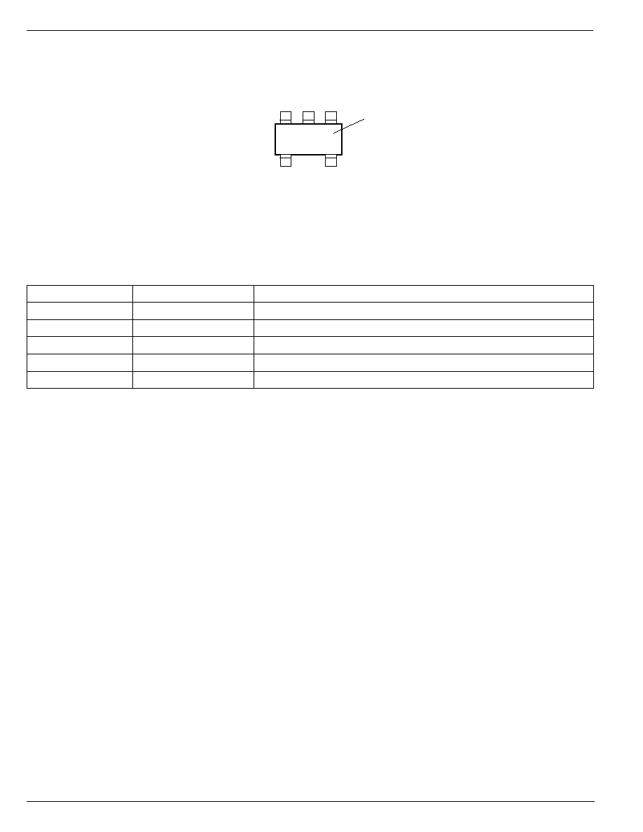
includes rail-to-rail input/output capabilities. The part is pack-
aged in the SOT-23-5 IttyBittyTM package.
The MIC7201 is designed using the MIC7101 operational
amplifier plus well-matched monolithic resistors to provide a
unity-gain stable differential input to signal-ended output
amplifier that requires a minimum of external components.
Performance is guaranteed from 2.2V through 10V.
Features
∑ Operates from 2.2V to 10V
∑
±
1% typical gain error
∑ 0.6mA typical supply current at 2.2V
∑ 400kHz bandwidth
∑ Small SOT-23-5 package
∑ Suitable for driving capacitive loads
Applications
∑ Cellular telephones
∑ Digital audio systems
∑ Mobile communications
∑ Portable computers and PDAs
Ordering Information
Part Number
Temperature Range
Package
MIC7201BM5
≠40
∞
C to +85
∞
C
SOT-23-5
Other voltages available. Contact Micrel for details.
Micrel, Inc. ∑ 1849 Fortune Drive ∑ San Jose, CA 95131 ∑ USA ∑ tel + 1 (408) 944-0800 ∑ fax + 1 (408) 944-0970 ∑ http://www.micrel.com
GainBlock is a trademark of Micrel, Inc.
Block Diagram
IN+
OUT
50k
100k
V+
50k
50k
100k
IN≠
V≠
MIC7201
1
2
3
4
5
Difference Amplifier Behavior
The desired 100mV, 400Hz differential sinusoidal signal is shown applied to
inputs V
IN≠
and V
IN+
. A 500mV, 5kHz square-wave "noise" signal is super-
imposed on both V
IN≠
and V
IN+
.
These signals demonstrate the noise cancellation ability of the MIC7201.
The output (V
OUT
) shows the recovered single-ended 200mV peak-to-peak,
400Hz sine wave.
V
IN≠
V
IN+
V
OUT
MIC7201
Micrel
MIC7201
2
December 1998
Pin Configuration
OUT
V+
IN≠
IN+
1
3
4
5
2
V≠
A16
Part
Identification
SOT-23-5
Pin Description
Pin Number
Pin Name
Pin Function
1
OUT
Amplifier Output: Single-ended output.
2
V+
Positive Supply: Positive power supply input.
3
IN+
Noniverting Input: In-phase differential input.
4
IN≠
Inverting Input: Out-of-phase differential input.
5
V≠
Ground: Power supply ground return.
December 1998
3
MIC7201
MIC7201
Micrel
Absolute Maximum Ratings
(Note 1)
Supply Voltage (V
V+
≠V
V≠
) ............................................. 12V
Differential Input Voltage (V
V+
≠V
V≠
) .................
±
(V
V+
≠V
V≠
)
I/O Pin Voltage (V
IN
, V
OUT
), Note 2
................................................ V
V≠
≠0.3V to V
V+
+0.3V
Junction Temperature (T
J
) ...................................... +150
∞
C
Storage Temperature (T
S
) ....................... ≠65
∞
C to +150
∞
C
Lead Temperature (soldering, 10 sec.) ..................... 260
∞
C
ESD, Note 5 .................................................................. 2kV
Operating Ratings
(Note 1)
Supply Voltage (V
V+
≠V
V≠
) ............................ +2.2V to +10V
Input Voltage (V
IN+
, V
IN≠
) ................................... V
V≠
to V
V+
Continuous Output Current ......................................
±
15mA
Junction Temperature (T
J
) ......................... ≠40
∞
C to +85
∞
C
Max. Junction Temperature (T
J(max)
), Note 3 ........... +85
∞
C
Package Thermal Resistance (
JA
), Note 4.......... 325
∞
C/W
Max. Power Dissipation ............................................ Note 3
Electrical Characteristics (2.2V)
V
V+
= 2.2V, V
V≠
= 0V, V
CM
= V
OUT
= V+/2; R
L
= 1M
; T
J
= 25
∞
C, bold values indicate ≠40
∞
C
T
J
+85
∞
C; unless noted
Symbol
Parameter
Condition
Min
Typ
Max
Units
E
Z
Zero Error
E
Z
=
V
OUT
≠ V
V+
/2
9
44
mV
TCV
OS
Input Offset Voltage Temp. Drift
14
µ
V/
∞
C
R
IN
Input Resistance
35
50
65
k
CMRR
Common-mode Rejection Ratio
V
CM
= 0V to V
V+
65
dB
±
PSRR
Split-Supply Rejection Ratio
V
V+
=
V
V≠
= 1.1V to 2.5V,
50
dB
V
CM
= 0V
+PSRR
Single-Supply Rejection Ratio,
V
V+
= 2.2V to 5V, V
V≠
= 0V, V
CM
= 1.1V
6
dB
Note 8
E
G
Gain Error, Note 9
0.2V
V
OUT
2.0V
±
1
%
V
OUT
Output Voltage Swing
output high, R
L
= 2k,
10
33
mV
Note 10
specified as V
V+
≠ V
OUT
50
mV
output low, R
L
= 2k
10
33
mV
50
mV
output high, R
L
= 600
,
33
mV
specified as V
V+
≠ V
OUT
mV
output low, R
L
= 600
33
mV
mV
I
SC
Output Short-Circuit Current
sinking or sourcing, Note 6, Note 7
20
60
mA
BW
Bandwidth
≠3dB point
400
kHz
SR
Slew Rate
0.5
V/
µ
s
THD
Total Harmonic Distortion
f = 1kHz
0.02
%
f = 10kHz
0.02
%
e
n
Input Referred Voltage Noise
f = 1kHz
30
nV Hz
/
I
S
Supply Current
no load
0.6
2.0
mA

MIC7201
Micrel
MIC7201
4
December 1998
Electrical Characteristics (5V)
V
V+
= +5V, V
V≠
= 0V, V
CM
= V
OUT
= V+/2; R
L
= 1M
; T
J
= 25
∞
C, bold values indicate ≠40
∞
C
T
J
+85
∞
C; unless noted
Symbol
Parameter
Condition
Min
Typ
Max
Units
E
Z
Zero Error
E
Z
=
V
OUT
≠ V
V+
/2
26
100
mV
TCV
OS
Input Offset Voltage Temp. Drift
14
µ
V/
∞
C
R
IN
Input Resistance
35
50
65
k
CMRR
Common-Mode Rejection Ratio
V
CM
= 0V to V
V+
65
dB
±
PSRR
Split-Supply Rejection Ratio
V
V+
=
V
V≠
= 2.5V to 5V,
50
dB
V
CM
= 0V
+PSRR
Single-Supply Rejection Ratio,
V
V+
= 5V to 10V, V
V≠
= 0V, V
CM
= 2.5V
6
dB
Note 8
E
G
Gain Error, Note 9
0.5V
V
OUT
4.5V
±
1
%
V
OUT
Output Voltage Swing
output high, R
L
= 2k,
15
50
mV
Note 10
specified as V
V+
≠ V
OUT
75
mV
output low, R
L
= 2k
15
50
mV
75
mV
output high, R
L
= 600
,
50
mV
specified as V
V+
≠ V
OUT
mV
output low, R
L
= 600
50
mV
mV
I
SC
Output Short-Circuit Current
sinking or sourcing, Note 6, Note 7
40
110
mA
BW
Bandwidth
≠3dB point
250
kHz
SR
Slew Rate
0.5
V/
µ
s
THD
Total Harmonic Distortion
f = 1kHz
0.02
%
f = 10kHz
0.02
%
e
n
Input Referred Voltage Noise
f = 1kHz
30
nV Hz
/
I
S
Supply Current
no load
0.8
2.8
mA
Electrical Characteristics (10V)
V
V+
= 10V, V
V≠
= 0V, V
CM
= V
OUT
= V+/2; R
L
= 1M
; T
J
= 25
∞
C, bold values indicate ≠40
∞
C
T
J
+85
∞
C; unless noted
Symbol
Parameter
Condition
Min
Typ
Max
Units
E
Z
Zero Error
E
Z
=
V
OUT
≠ V
V+
/2
60
200
mV
TCV
OS
Input Offset Voltage Temp. Drift
14
µ
V/
∞
C
R
IN
Input Resistance
35
50
65
k
CMRR
Common-Mode Rejection Ratio
V
CM
= 0V to V
V+
65
dB
±
PSRR
Split-Supply Rejection Ratio
V
V+
=
V
V≠
= 2.5V to 5V,
50
dB
V
CM
= 0V
+PSRR
Single-Supply Rejection Ratio,
V
V+
= 5V to 10V, V
V≠
= 0V, V
CM
= 2.5V
6
dB
Note 8
E
G
Gain Error, Note 9
0.5V
V
OUT
9.5V
±
1
%

December 1998
5
MIC7201
MIC7201
Micrel
Symbol
Parameter
Condition
Min
Typ
Max
Units
V
OUT
Output Voltage Swing
output high, R
L
= 2k,
24
80
mV
Note 10
specified as V
V+
≠ V
OUT
120
mV
output low, R
L
= 2k
24
80
mV
120
mV
output high, R
L
= 600
,
80
mV
specified as V
V+
≠ V
OUT
mV
output low, R
L
= 600
80
mV
mV
I
SC
Output Short-Circuit Current
sinking or sourcing, Note 6, Note 7
40
200
mA
BW
Bandwidth
≠3dB point
250
kHz
SR
Slew Rate
0.5
V/
µ
s
THD
Total Harmonic Distortion
f = 1kHz
0.02
%
f = 10kHz
0.02
%
e
n
Input Referred Voltage Noise
f = 1kHz
30
nV Hz
/
I
S
Supply Current
no load
1.2
4.0
mA
Internal Op Amp Typical Characteristics
+2.2V
V
V+
10V, V
V≠
= 0V, V
CM
= V
OUT
= V+/2; R
L
= 1M
; T
J
= 25
∞
C, bold values indicate ≠40
∞
C
T
J
+85
∞
C; unless noted
Symbol
Parameter
Condition
Min
Typ
Max
Units
V
OS
Input Offset Voltage
0.11
mV
TCV
OS
Input Offset Voltage Drift
1.0
µ
V/
∞
C
I
B
Input Bias Current
1.0
pA
I
OS
Input Offset Current
0.5
pA
R
IN
Input Resistance
>1
T
CMRR
Common-Mode Rejection Ratio
0V
V
CM
V
V+
80
dB
V
CM
Input Common-Mode Voltage
input low
≠0.3
V
input high
V
V+
+0.3
V
PSRR
Power Supply Rejection Ratio
V
V+
=
V
V≠
= 1.1V to 1.65V,
60
dB
V
CM
= 0V
General Note: Devices are ESD protected; however, handling precautions are recommended. All limits guaranteed by testing or statistical analysis.
Note 1:
Absolute maximum ratings indicate limits beyond which damage to the component may occur. Electrical specifications do not apply when
operating the device outside its recommended operating ratings.
Note 2:
I/O pin voltage is any external voltage to which an input or output is referenced.
Note 3:
The maximum allowable power dissipation is a function of the maximum junction temperature, T
J(max)
; the junction-to-ambient thermal
resistance,
JA
; and the ambient temperature, T
A
. The maximum allowable power dissipation at any ambient temperature is calculated using:
P
D
= (T
J(max)
≠ T
A
) /
JA
. Exceeding the maximum allowable power dissipation will result in excessive die temperature.
Note 4:
Thermal resistance,
JA
, applies to a part soldered on a printed-circuit board.
Note 5:
Human body model, 1.5k in series with 100pF.
Note 6:
Short circuit may cause the device to exceed maximum allowable power dissipation. See Note 3.
Note 7:
Shorting V
OUT
to V+ when V+ > 10V may damage the device.
Note 8:
Limited by internal bias-network resistors. Power supply must be "clean." Power supply should be bypassed as shown in typical application
circuit.
Note 9:
The gain error specification applies to differential, inverting, and noninverting gains.
Note 10: Since the part is specified in a single-supply configuration, the output load (R
L
) is a Thevenin equivalent value. The actual load consists of 2
◊
R
L
to ground and 2
◊
R
L
to the supply (V+).