
August 1, 2000
1
MIC74
MIC74
Micrel
MIC74
2-Wire Serial I/O Expander and Fan Controller
Advance Information
General Description
The MIC74 is a fully programmable serial-to-parallel I/O
expander compatible with the SMBusTM (system manage-
ment bus) protocol. It acts as a "slave" on the bus, providing
eight independent I/O lines.
Each I/O bit can be individually programmed as an input or
output. If programmed as an output, each I/O bit can be
programmed as an open-drain or complementary push-pull
output. If desired, the four most significant I/O bits can be
programmed to implement fan speed control. An internal
clock generator and state machine eliminate the overhead
generally associated with "bit-banging" fan speed control.
Programming the device and reading/writing the I/O bits is
accomplished using seven internal registers. All registers can
be read by the host. Output bits are capable of directly driving
high-current loads such as LEDs. A separate interrupt output
can notify the host of state changes on the input bits without
requiring the MIC74 to perform a transaction on the serial bus
or be polled by the host. Three address selection inputs are
provided, allowing up to eight devices to share the same bus
and provide a total of 64 bits of I/O.
The MIC74 is available in an ultra-small-footprint 16-lead
QSOP. Low quiescent current, small footprint, and low pack-
age height make the MIC74 ideal for portable and desktop
applications.
Typical Application
R1
LED1
LED8
R9
R2
R3
R4
R5
R6
R7
R8
3.0V
3.0V
VDD
/ALERT
DATA
CLK
ALERT
DATA
CLK
A0
A1
A2
GND
P0
P1
P2
P3
P4
P5
P6
P7
MIC74
Serial-Bus-Controlled LED Annunciator
Features
� Provides eight bits of general purpose I/O
� Built in fan speed control logic (optional)
� 2-wire SMBusTM/I
2
CTM compatible serial interface
plus interrupt output
� 2.7V to 3.6V operating voltage range
� 5V-tolerant I/O
� Low quiescent current: 2
�A (typical)
� Bit-programmable I/O options:
input or output
push-pull or open-drain output
interrupt on input changes
� Outputs can directly drive LEDs (10mA I
OL
)
� Up to 8 devices per bus
Applications
� General purpose I/O expansion via serial bus
� Personal computer system management
� Distributed sensing and control
� Microcontroller I/O expansion
� Fan Control
Ordering Information
Part Number
Temperature Range
Package
MIC74BQS
�40
�C to +85�C
16-lead QSOP
Micrel, Inc. � 1849 Fortune Drive � San Jose, CA 95131 � USA � tel + 1 (408) 944-0800 � fax + 1 (408) 944-0970 � http://www.micrel.com
SMBusTM is a trademark of Intel Corporation. I
2
CTM is a trademark of Phillips Electronics N.V.

MIC74
Micrel
MIC74
2
August 1, 2000
Pin Description
Pin Number
Pin Name
Pin Function
1�3
A0�A2
Address (Input): Slave address selection inputs; sets the three least signifi-
cant bits of the MIC74's slave address.
4�7
P0�P3
Parallel I/O (Input/Output): General-purpose I/O pin. Direction and output
type are user programmable.
8
GND
Ground
9�12
P4�P7 (/SHDN, /FS0�/FS2)
Parallel I/O (Input/output): P4�P7 are general-purpose I/O pins. Direction
and output type are user programmable.
Shutdown (Output): When the FAN bit is set, pin 9 becomes SHDN.
Fan Speed (Output): When the FAN bit is set, pins 10 through 12 become /
FS0�/FS2 respectively, controlled by the FAN_SPEED register.
13
/ALERT
Interrupt (Output): Active-low, open-drain output signals input-change-
interrupts to the host on this pin. Signal is cleared when the bus master
(host) polls the ARA (alert response address = 0001 100) or reads status.
14
CLK
Serial Bus Clock (Input): The host provides the serial bit clock in this input.
15
DATA
Serial Data (Input/Output): Serial data input and open-drain serial data
output.
16
VDD
Power Supply (Input.)
Pin Configuration
1
A0
A1
A2
P0
P1
P2
P3
GND
16 VDD
DATA
CLK
/ALERT
P7 (/FS2)
P6 (/FS1)
P5 (/FS0)
P4 (/SHDN0)
15
14
13
12
11
10
9
2
3
4
5
6
7
8
16-Lead QSOP

August 1, 2000
3
MIC74
MIC74
Micrel
Absolute Maximum Ratings
(Note 1)
Supply Voltage (V
DD
) ................................................. +4.6V
Input Voltage
[all pins except
V
DD
and GND] (V
IN
) ........................ GND � 0.3V to 5.5V
Junction Temperature (T
J
) ...................................... +150
�C
Lead Temperature (10 sec.) .................................... +260
�C
ESD Rating, Note 3
V
DD ...........................................................................................
1.5kV
A0,A1,A2 ................................................................. 500V
Others ..................................................................... 200V
Operating Ratings
(Note 2)
Supply Voltage (V
DD
) .................................. +2.7V to +3.6V
Ambient Temperature (T
A
) ......................... �40
�C to +85�C
Package Thermal Resistance ............................... 163
�C/W
Electrical Characteristics
2.7V
V
DD
3.6V; T
A
= 25
�C, bold values indicate �40�C T
A
+85�C; unless noted.
Symbol
Parameter
Condition
Min
Typ
Max
Units
V
IN
Input Voltage, any pin except
GND�0.3
5.5
V
V
DD
and GND
I
DD
Operating Supply Current
P[7:0] inputs; P[7:0] = V
DD
or GND
2
6
�A
/ALERT open; f
CLK
= 100kHz
I
START
Fan Startup Supply Current
during t
START
;
/ALERT, /SHDN,
1.75
mA
(Fan Mode Only)
/FS2[2:0] = open; V
SMBCLK
= V
SMBDATA
= V
DD
;
P[3:0] = inputs
I
STBY
Standby Supply Current
/ALERT = open, V
SMBCLK
= V
SMBDATA
= V
DD
;
1
3
�A
P[3:0] = inputs
Serial I/O (DATA, CLK)
V
IL
Input Low Voltage
�0.3
0.8
V
V
IH
Input High Voltage
2.0
5.5
V
V
OL
Output Low Voltage
I
OL
= 3mA
0.4
V
I
LEAK
Leakage Current
V
IN
= 5.5V
or GND
�1
+1
�A
C
IN
Input Capacitance
10
pF
Parallel I/O [P0�P3, P4(/SHDN), P5(/FS0)�P7(/FS2)]
V
IL
Input Low Voltage
�0.5
0.8
V
V
IH
Input High Voltage
2
5.5
V
I
OL
Output Low Current
V
OL
= 0.4V, V
DD
= 2.7V
7
mA
V
OL
= 1V, V
DD
= 3.3V
10
mA
I
OH
Output High Current
V
OH
= 2.4V
7
mA
I
LEAK
Leakage Current
V
IN
= 5.5V
or GND
�1
+1
�A
C
IN
Input Capacitance
10
pF
C
OUT
Output Capacitance
10
pF
Address Input (A0�A2)
V
IL
Input Low Voltage
�0.3
0.3V
DD
V
V
IH
Input High Voltage
0.7V
DD
V
DD
+0.3
V
I
LEAK
Leakage Current
V
IN
= V
DD
or GND
�250
+250
nA

MIC74
Micrel
MIC74
4
August 1, 2000
Symbol
Parameter
Condition
Min
Typ
Max
Units
/ALERT
V
OL
Output Low Voltage
I
OL
= 1mA
0.4
V
I
LEAK
Leakage Current
V
IN
= V
DD
or V
SS
�1
�250
+1
�A
AC Characteristics
t
START
Fan Startup Interval
normal operation
0.5
1
3.3
sec
t
PULSE
Minimum Pulse-Width
minimum pulse-width on P
n to
10
ns
generate an interrupt, Note 7
t
/INT
Interrupt Delay
interrupt delay from state change
4
�s
on P
n to /ALERT
V
OL
, Note 7
t
/IR
Delay from Status Read or ARA
4
�s
Response to /ALERT
V
OH
t
HD:STA
Hold Time, Note 7
hold time after repeated start condition.
4.0
�s
after this period, the first clock is generated.
t
SU:STA
Setup Time, Note 7
repeated start condition setup time
4.7
�s
t
SU:STO
Stop Condition Setup Time
Note 7
4.0
�s
t
HD:DAT
Data Hold Time
Note 7
500
ns
t
SU:DAT
Data Setup Time
Note 7
0
ns
t
TIMEOUT
Clock Low Time-Out
Notes 4, 7
25
35
ms
t
LOW
Clock Low Period
Notes 5, 7
4.7
�s
t
HIGH
Clock High Period
Notes 5, 7
4.0
50
�s
t
F
Clock/Data Fall Time
Notes 6, 7
300
ns
t
R
Clock/Data Rise Time
Notes 6, 7
1000
ns
t
BUF
Bus free time between stop and
Note 7
4.7
�s
Start condition
Note 1.
Exceeding the absolute maximum rating may damage the device.
Note 2.
The device is not guaranteed to function outside its operating rating.
Note 3.
Devices are ESD sensitive. Handling precautions recommended. Human body model, 1.5k in series with 100pF.
Note 4.
Devices participating in a transfer will timeout when any clock low exceeds the value of t
TIMEOUT(min)
of 25ms. Devices that have detected a
timeout condition must reset the communication no later than t
TIMEOUT(max)
of 35ms. The maximum value specified must be adhered to by
both a master and a slave as it incorporates the cumulative stretch limit for both a master (10ms) and a slave (25ms).
Note 5.
t
HIGH(max)
provides a simple guaranteed method for devices to detect bus idle conditions.
Note 6.
Rise and fall time is defined as follows: t
R
= V
IL(max)
� 0.15V to V
IH(min)
+ 0.15V; t
F
= 0.9V
DD
to V
IL(max)
� 0.15V.
Note 7.
Guaranteed by design.
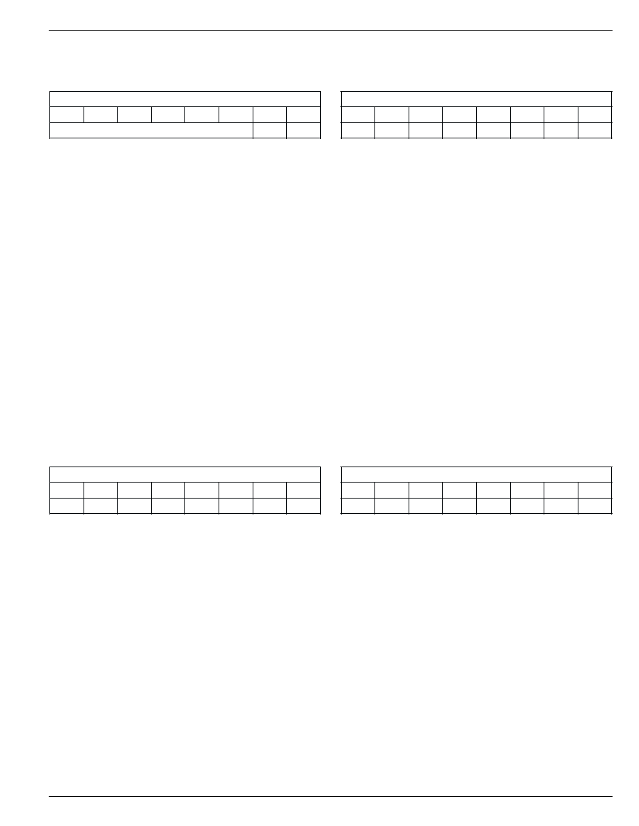
Timing Definitions
DATA
CLK
t
R
t
F
t
HD:STA
t
SU:STO
t
HD:DAT
t
HD:STA
t
SU:DAT
t
HIGH
t
SU:STA
t
BUF
t
LOW
StoP
StoP
Start
Start
August 1, 2000
5
MIC74
MIC74
Micrel
Register Descriptions
Device Configuration Register
G
F
C
_
V
E
D
]
7
[
D
]
6
[
D
]
5
[
D
]
4
[
D
]
3
[
D
]
2
[
D
]
1
[
D
]
0
[
D
.
o
r
e
z
s
a
e
t
i
r
w
s
y
a
w
l
A
N
A
F
E
I
Power-On Default Value: 0000 0000
b
, 00
h
Interrupts disabled
Not in Fan Mode
Command_byte addess: 0000 0000
b
, 00
h
Type:
8-bits, read/write
Bit Name:
IE
Function:
Global interrupt enable.
Operation: 1 = enabled
0 = disabled
Bit Name:
FAN
Function:
Selects Fan Mode
(P[7:4] vs. /FS[2:0], /SHDN)
Operation: 1 = Fan Mode
0 = I/O Mode
Bit Name:
D[2] through D[6]
Function:
Reserved
Operation: Reserved--always write as zero
Data Direction Register
R
I
D
]
7
[
D
]
6
[
D
]
5
[
D
]
4
[
D
]
3
[
D
]
2
[
D
]
1
[
D
]
0
[
D
7
R
I
D
6
R
I
D
5
R
I
D
4
R
I
D
3
R
I
D
2
R
I
D
1
R
I
D
0
R
I
D
Power-On Default Value: 0000 0000
b
, 00
h
all P
n's configured as inputs
Command_byte addess: 0000 0001
b
, 01
h
Type:
8-bits, read/write
Bit Name:
DIR
n
Function:
Selects data direction, input or output, of P
n
Operation: 1 = output
0 = input
Notes:
If Fan Mode is selected, that is, the FAN bit of
the DEV_CFG register is set to one, P[7:4] are
automatically configured as open-drain
outputs. They are then referred to as /FS[2:0]
and /SHDN. The DIR register has no effect on
these I/O bits while in Fan Mode.
Output Configuration Register
G
F
C
_
T
U
O
]
7
[
D
]
6
[
D
]
5
[
D
]
4
[
D
]
3
[
D
]
2
[
D
]
1
[
D
]
0
[
D
7
T
U
O
6
T
U
O
5
T
U
O
4
T
U
O
3
T
U
O
2
T
U
O
1
T
U
O
0
T
U
O
Power-On Default Value: 0000 0000
b
, 00
h
all outputs open-drain
Command_byte addess: 0000 0010
b
, 02
h
Type:
8-bits, read/write
Bit Name:
OUT
n
Function:
Selects output driver configuration of P
n when
P
n is configured as an output.
Operation: 1 = push-pull
0 = open-drain
Notes:
If Fan Mode is selected, that is, the FAN bit of
the DEV_CFG register is set to one, P[7:4] are
automatically configured as open-drain
outputs. They are then referred to as /FS[2:0]
and /SHDN. The OUT_CFG register has no
effect on these I/O bits while in Fan Mode.
Status Register
S
U
T
A
T
S
]
7
[
D
]
6
[
D
]
5
[
D
]
4
[
D
]
3
[
D
]
2
[
D
]
1
[
D
]
0
[
D
7
S
6
S
5
S
4
S
3
S
2
S
1
S
0
S
Power-On Default Value: 0000 0000
b
, 00
h
no interrupts pending
Command_byte addess: 0000 0011
b
, 03
h
Type:
8-bits, read only
Bit Name:
S
n
Function:
Flag for Pn input-change event when P
n is
configured as an input; S
n is set when the
corresponding input changes state.
Operation: 1 = change occured
0 = no change occured
Notes:
If Fan Mode is selected, that is, the FAN bit of
the DEV_CFG register is set to one, P[7:4] are
automatically configured as open-drain
outputs. They are then referred to as /FS[2:0]
and /SHDN. No interrupts of any kind are
generated by these pins while in Fan Mode.
All status bits are cleared after any read
operation is performed on STATUS.