June 2000
1
MIC79050
MIC79050
Micrel
Typical Applications
Li-Ion
Cell
4.2V
±
0.75% Over Temp
IN
BAT
GND
MIC79050-4.2BS
Regulated or
unregulated
wall adapter
Simplest Battery Charging Solution
4.2V
±
0.75%
Li-Ion
Cell
IN
BAT
FB
GND
EN
MIC79050-4.2BMM
External PWM*
*See Applications Information
Regulated or
unregulated
wall adapter
Pulse-Charging Application
MIC79050
Simple Lithium-Ion Battery Charger
Preliminary Information
General Description
The MIC79050 is a simple single-cell lithium-ion battery
charger. It includes an on-chip pass transistor for high preci-
sion charging. Featuring ultrahigh precision (+0.75% over the
Li-ion battery charging temperature range) and "zero" off
mode current, the MIC79050 provides a very simple, cost
effective solution for charging lithium-ion battery.
Other features of the MIC79050 include current limit and
thermal shutdown protection. In the event the input voltage to
the charger is disconnected, the MIC79050 also provides
minimal reverse-current and reversed-battery protection.
The MIC79050 is a fixed 4.2V device and comes in the
thermally-enhanced MSO-8, SO-8, and SOT-223 packages.
The 8-pin versions also come equipped with enable and
feedback inputs. All versions are specified over the tempera-
ture range of ≠40
∞
C to +125
∞
C.
Features
∑ High accuracy charge voltage:
±
0.75% over -5
∞
C to + 60
∞
C (Li-ion charging
temperature range)
∑ "Zero" off-mode current
∑ 10
µ
A reverse leakage
∑ Ultralow 380mV dropout at 500mA
∑ Wide input voltage range
∑ Logic controlled enable input (8-pin devices only)
∑ Thermal shutdown and current limit protection
∑ Power MSOP-8, Power SOP-8, and SOT-223
∑ Pulse charging capability
Applications
∑ Li-ion battery charger
∑ Celluar phones
∑ Palmtop computers
∑ PDAs
∑ Self charging battery packs
Micrel, Inc. ∑ 1849 Fortune Drive ∑ San Jose, CA 95131 ∑ USA ∑ tel + 1 (408) 944-0800 ∑ fax + 1 (408) 944-0970 ∑ http://www.micrel.com
Ordering Information
Part Number
Voltage
Junct. Temp. Range
Package
MIC79050-4.2BS
4.2V
≠40
∞
C to +125
∞
C
SOT-223
MIC79050-4.2BM
4.2V
≠40
∞
C to +125
∞
C
SOP-8
MIC79050-4.2BMM
4.2V
≠40
∞
C to +125
∞
C
MSOP-8
June 2000
3
MIC79050
MIC79050
Micrel
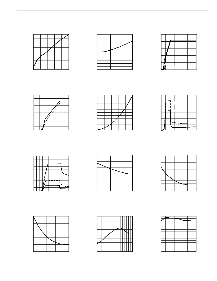
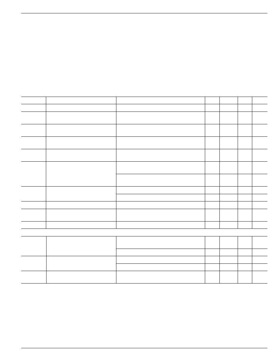
Electrical Characteristics
V
IN
= V
BAT
+ 1.0V; C
OUT
= 4.7
µ
F, I
OUT
= 100
µ
A; T
J
= 25
∞
C, bold values indicate ≠40
∞
C
T
J
+125
∞
C; unless noted.
Symbol
Parameter
Conditions
Min
Typical
Max
Units
V
BAT
Battery Voltage Accuracy
variation from nominal V
OUT
≠5
∞
C to +60
∞
C
≠0.75
+0.75
%
V
BAT
/
T
Battery Voltage
Note 4
40
ppm/
∞
C
Temperature Coefficient
V
BAT
/V
BAT
Line Regulation
V
IN
= V
BAT
+ 1V to 16V
0.009
0.05
%/V
0.1
%/V
V
BAT
/V
BAT
Load Regulation
I
OUT
= 100
µ
A to 500mA, Note 5
0.05
0.5
%
0.7
%
V
IN
≠ V
BAT
Dropout Voltage, Note 6
I
OUT
= 500mA
380
500
mV
600
mV
I
GND
Ground Pin Current, Notes 7, 8
V
EN
3.0V, I
OUT
= 100
µ
A
85
130
µ
A
170
µ
A
V
EN
3.0V, I
OUT
= 500mA
11
20
mA
25
mA
I
GND
Ground Pin Quiescent Current,
V
EN
0.4V (shutdown)
0.05
3
µ
A
Note 8
V
EN
0.18V (shutdown)
0.10
8
µ
A
PSRR
Ripple Rejection
f = 120Hz
75
dB
I
LIMIT
Current Limit
V
BAT
= 0V
750
900
mA
1000
mA
V
BAT
/
P
D
Thermal Regulation
Note 9
0.05
%/W
ENABLE Input
V
ENL
Enable Input Logic-Low Voltage
V
EN
= logic low (shutdown)
0.4
V
0.18
V
V
EN
= logic high (enabled)
2.0
V
I
ENL
Enable Input Current
V
ENL
0.4V (shutdown)
0.01
≠1
µ
A
V
ENL
0.18V (shutdown)
0.01
≠2
µ
A
I
ENH
V
ENH
2.0V (enabled)
5
20
µ
A
25
µ
A
Note 1.
Exceeding the absolute maximum rating may damage the device.
Note 2.
The device is not guaranteed to function outside its operating rating.
Note 3.
The maximum allowable power dissipation at any T
A
(ambient temperature) is calculated using: P
D(max)
= (T
J(max)
≠ T
A
)
˜
JA
. Exceeding the
maximum allowable power dissipation will result in excessive die temperature, and the regulator will go into thermal shutdown.
Note 4.
Battery voltage temperature coefficient is the worst case voltage change divided by the total temperature range.
Note 5.
Regulation is measured at constant junction temperature using low duty cycle pulse testing. Parts are tested for load regulation in the load
range from 100
µ
A to 500mA. Changes in output voltage due to heating effects are covered by the thermal regulation specification.
Note 6.
Dropout voltage is defined as the input to battery output differential at which the battery voltage drops 2% below its nominal value measured at
1V differential.
Note 7:
Ground pin current is the charger quiescent current plus pass transistor base current. The total current drawn from the supply is the sum of the
load current plus the ground pin current.
Absolute Maximum Ratings
(Note 1)
Supply Input Voltage (V
IN
) ............................ ≠20V to +20V
Power Dissipation (P
D
) ............... Internally Limited, Note 3
Junction Temperature (T
J
) ....................... ≠40
∞
C to +125
∞
C
Lead Temperature (soldering, 5 sec.) ....................... 260
∞
C
Storage Temperature (T
S
) ....................... ≠65
∞
C to +150
∞
C
Operating Ratings
(Note 2)
Supply Input Voltage (V
IN
) ........................... +2.5V to +16V
Enable Input Voltage (V
EN
) .................................. 0V to V
IN
Junction Temperature (T
J
) ....................... ≠40
∞
C to +125
∞
C
Package Thermal Resistance (Note 3) ...............................
MSOP-8 (
JA
) ...................................................... 80
∞
C/W
SOP-8(
JA
) .......................................................... 63
∞
C/W
SOT-223(
JC
) ...................................................... 15
∞
C/W