MPD8021
Micrel
11-4
1997
MPD8021
e
TM Semicustom High-Voltage Array
Summary Information
General Description
The MPD8021 is a semicustom, high-voltage, mixed-mode,
power ASIC (Application Specific Integrated Circuit) suitable
for quantities from 10 to 100,000's of pieces. Clients can
begin designing proprietary ASICs using a low-cost SPICE
simulator and the free MPD8021 Design Kit--available for
downloading via the Internet.
Technology
The MPD8021 features bipolar/CMOS/DMOS high-voltage
technology and is fabricated using Micrel's proprietary BCD5
process to combine high-speed, low-voltage digital and ana-
log circuits with high-voltage DMOS power drive circuits on a
single chip.
All logic and analog circuitry is powered from a single +3V to
+12V supply. The high-voltage portion functions at voltages
from +20V to over +100V and includes a charge pump.
Rapid Turnaround
Micrel delivers rapid turnaround by applying a unique metal
interconnect pattern, based on the client's design, to a stock
MPD8021 wafer.
To facilitate a rapid and low-cost design
approach, Micrel offers MPD8021 development programs
that range from limited assistance to full turnkey.
When you are ready for production, count on Micrel's proven
fab and test group to provide timely deliveries of high-quality,
fully-tested, proprietary ICs.
Low-Cost Development
There is no cost or obligation to begin developing your own
MPD8021-based custom IC. "Kit parts" which are actual
working designs, featuring access to many internal functions,
are available for breadboarding circuits.
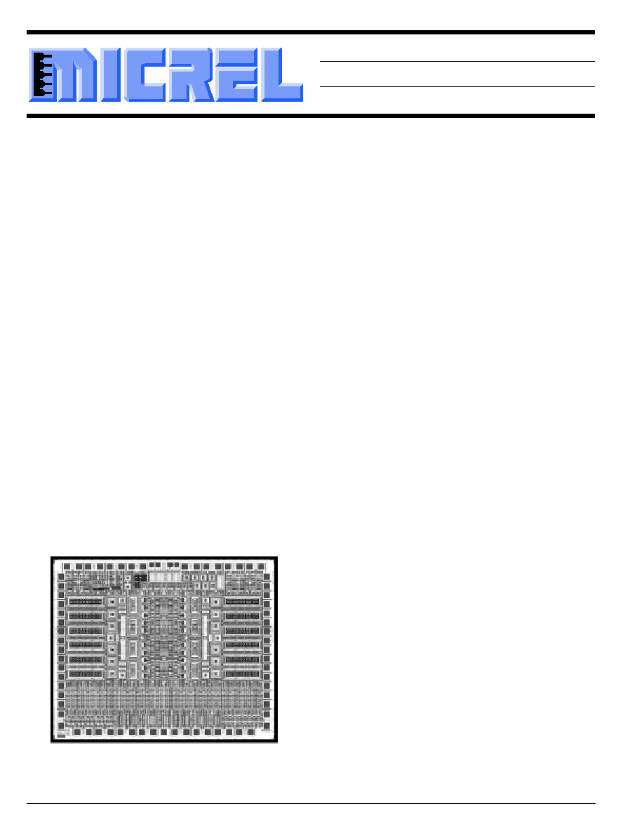
MPD8021 Die (0.192"
◊
0.200")
Features
∑ 12 N-channel, 100V, 200mA, 10
,
fully-floating DMOS power FETs
(can be paralleled for 100V, 2.4A, 0.83
single,
half-bridge, or bilateral switches)
∑ 40 high-voltage PMOS FETs
(for level shifting, high-voltage amplifiers)
∑ 12 high-voltage 200
, DMOS FETs
(for level shifting, voltage amplifiers)
∑ 20 high-voltage, grounded-source,
DMOS FETs
(for level shifting, current mirrors)
∑ >100 uncommitted CMOS gates
∑ 12 CMOS/TTL I/O buffers
∑ 13 low-voltage CMOS tile arrays
(for op amps, comparators, digital circuitry)
∑ 14 dual-collector PNPs and 12 NPNs
(for trimmed bandgaps, low-offset amplifiers or com-
parators, temperature sensor)
∑ 3-bit trimming network
(for production trimmed bandgaps or offsets)
∑ High- and low-value resistors and capacitors
(>1M
total resistance, 45pF total capacitance)
∑ 12V and 6V zener diodes
(gate-to-source clamps, voltage references)
∑ 67 I/O pads
(36 include 2kV ESD protection)
∑ Guaranteed ≠55
∞
C to +150
∞
C operation
∑ Several package options
∑ Low-cost prototyping program
∑ Design support via Internet
Applications
∑ 2
and 3
motor control
∑ High-voltage, controlled-slew, bus drivers
∑ High-voltage display drivers
∑ Lamp drivers with current limit and
overtemperature protection
∑ Relay and solenoid drivers
∑ Half- and full-bridge drivers
∑ Multioutput switching power supplies
∑ High-voltage linear power supplies
∑ High-voltage signal processing
MPD8021 World-Wide Web Site
∑ http://www.micrel.com
-- select "
e
" or
"Custom Solutions"
∑ e-mail: help@ezanalog.com

1997
11-5
MPD8021
Micrel
11
Absolute Maximum Ratings
DC Input Voltage
Negative, Any Pin (V
IL
), Note 1 .................. V
SUB
≠ 0.5V
DC Input Voltage
Positive ESD Pin (V
IH
), Note 2 ........................ V
+
+ 0.5V
Low-Voltage Supply Differential, Note 3 .................. +16.5V
DMOS Output Device Breakdown (BV
DSS
), Note 4 . +110V
DMOS Drain Current
Continuous (I
D(max)
), Note 5 .................................... 0.2A
Pulsed (I
D(pulse)
), Note 6 .......................................... 0.5A
DMOS Gate Drive Voltage (V
GS(max)
), Note 7 ............
±
20V
Standard ESD Structure Voltage (V
ESD
), Note 8 .......... 2kV
Storage Temperature (T
S
) ....................... ≠65
∞
C to +150
∞
C
General Note: Devices are ESD protected; however, handling precau-
tions are recommended.
Note 1:
V
SUB
is the substrate bias voltage.
Note 2:
V
+
is the positive ESD clamp potential, user specificed up to
+100V.
Note 3:
Maximum voltage across low-voltage analog or digital MOS.
Note 4:
DMOS source-to-body shorted to substrate at 0V.
Note 5:
V
GS
= 15V.
Note 6:
5
µ
s pulse, 10% duty cycle.
Note 7:
Measured relative to source-to-body short.
Note 8:
Measured between any two pins.
Operating Ratings
Ambient Temperature (T
A
) ....................... ≠55
∞
C to +125
∞
C
Electrical and Physical Summary
Bonding Pads .................................................................. 67
2kV ESD Pads ................................................................ 36
Die Size ............................................... 0.222 in.
◊
0.182 in.
CMOS Output Buffer Tiles .............................................. 12
CMOS Analog Tiles ......................................................... 13
High-Power DMOS ................................................ 12@10
Bipolar Devices
split-collector PNP ....................................................... 14
NPN ............................................................................. 14
zener diodes ................................................................ 10
CMOS Logic Devices
NMOS ....................................................................... 354
PMOS ........................................................................ 354
Resistance
P-well ...................................................................... 1M
N+ ............................................................................ 20k
polysilicon ....................................................... up to 50k
Capacitance ................................................................ 45pF
Trimming Range ......................................................... 3 bits
MPD8021-0002 Kit Part
High-Voltage Characterization Array
High-voltage NPN transistors ............................................ 4
(includes matching pair)
High-voltage PNP transistor .............................................. 1
High-voltage P-channel FETs ........................................... 2
Analog and digital low-voltage MOSFETs ......................... 8
Expitaxial JFET ................................................................. 1
200
and 10
high-voltage DMOS transistors ................. 3
6V and 12V Zener diodes ................................................. 2
Small Schottky diode ......................................................... 1
ESD input protection structures ........................................ 2
High-value resistor (100k) ................................................. 1
Low-value resistor (7.6k) ................................................... 1
Low-value polysilicon resistor ........................................... 1
This device is suitable for curve tracer or bench-top characterization of
various device types included in the MPD8021 array. This device is a
supplement to the design information available in the Internet Design
Kit.
MPD8021-0001 Kit Part
High-Voltage PWM Controller
High-voltage push-pull output stages ................................ 6
with CMOS to high-voltage level shifters
and crossover protection logic
High-voltage charge pump for high-side drive
with integral high-side current mirror
Bandgap reference ............................................................ 1
with PTAT voltage output
(usable for thermal shutdown)
Op amp ............................................................................. 1
Comparators ..................................................................... 4
Floating logic input
Undervoltage lockout
Digital cells and miscellaneous components are not accessible from
the pins of this device.
Ordering Information
Part Number
Type
Temperature Range
Package
MIC8021-xxxx*
custom
≠55
∞
C to +125
∞
C
customer specified
MIC8021-0001
kit part
≠55
∞
C to +125
∞
C
68-pin PLCC
MIC8021-0002
kit part
≠55
∞
C to +125
∞
C
68-pin PLCC
* custom part number. Package markings customer specificed.