December 2000
1
MIC820
MIC820
Micrel
MIC820
TeenyTM Ultra Low Power Op Amp
Final Information
General Description
The MIC820 is a rail-to-rail output, operational amplifier in
TeenyTM SC70 packaging. The MIC820 provides 5MHz, -3dB
bandwidth while consuming an incredibly low 22
µ
A supply
current.
The SC70 packaging achieves significant board space sav-
ings over devices packaged in SOT-23 or MSOP-8 packag-
ing. The SC70 occupies approximately half the board area of
a SOT-23 package.
Features
∑
TeenyTM SC70 packaging
∑ 5MHz, ≠3dB bandwidth product
∑ 4MHz gain-bandwidth product
∑ 22
µ
A supply current
∑ Rail-to-Rail output
∑ Ground sensing at input common mode to GND
∑ Common mode to GND
∑ Drive large capactive loads
Applications
∑ Portable equipment
Micrel, Inc. ∑ 1849 Fortune Drive ∑ San Jose, CA 95131 ∑ USA ∑ tel + 1 (408) 944-0800 ∑ fax + 1 (408) 944-0970 ∑ http://www.micrel.com
Pin Configuration
OUT
V+
IN≠
IN+
1
3
4
5
2
V≠
A25
Part
Identification
SC-70
Functional Pinout
OUT
V+
IN≠
IN+
1
3
4
5
2
V≠
Ordering Information
Part Number
Marking
Junction Temp. Range*
Package
MIC820BC5
A25
≠40
∞
C to +85
∞
C
SC70-5
Teeny is a trademark of Micrel, Inc.

MIC820
Micrel
MIC820
2
December 2000
Absolute Maximum Ratings
(Note 1)
Supply Voltage (V
V+
≠ V
V≠
) ........................................ +6.0V
Differentail Input Voltage (
V
IN+
≠ V
IN≠
) ................. +6.0lV
Input Voltage (V
IN+
≠ V
IN≠
) .............. V
V+
+ 0.3V, V
V≠
≠0.3V
Lead Temperature (soldering, 5 sec.) ....................... 260
∞
C
Output Short Circuit Current Duration .................. Indefinite
Storage Temperature (T
S
) ........................................ 150
∞
C
ESD Rating, Note 3
Operating Ratings
(Note 2)
Supply Voltage (V
S
) ................................ +4.75V to +5.25V
Ambient Temperature Range ..................... ≠40
∞
C to +85
∞
C
Package Thermal Resistance ............................... 450
∞
C/W
Electrical Characteristics (0V to 5V)
V
V+
= +5V, V
V≠
= 0V, V
CM
= V+/2; R
L
= 1M
; T
A
= 25
∞
C, bold values indicate ≠40
∞
C
T
A
+85
∞
C; unless noted.
Symbol
Parameter
Condition
Min
Typ
Max
Units
V
OS
Input Offset Voltage
1
15
mV
Input Offset Voltage Temp Coefficient
13
µ
V/
∞
C
I
B
Input Bias Current
0.165
5
nA
I
OS
Input Offset Current
0.1
5
nA
V
CM
Input Voltage Range
CMRR > 35dB
0
V
CC
-2.5
V
CMRR
Common-Mode Rejection Ratio
0 < V
CM
< 2.5V
35
50
dB
PSRR
Power Supply Rejection Ratio
Note 5
40
70
dB
A
VOL
Large-Signal Voltage Gain
R
L
= 1M, ≠0.5 < V
OUT
< 3.5V
60
72
dB
V
OUT
Maximum Output Voltage Swing
R
L
= 200k
4.95
5
V
V
OUT
Minimum Output Voltage Swing
R
L
= 200k
0
50
mV
BW
≠3db Bandwidth
5
MHz
GBW
Gain-Bandwidth Product
4
MHz
SR
Slew Rate
5
V/
µ
s
I
SC
Short-Circuit Output Current
Source
2
2.85
mA
Sink
0.15
0.26
mA
I
GND
Supply Current
V
CC
=
±
2.5V, V
OUT
= 0V
22
35
µ
A
V
CC
=
±
2.5V, V
OUT
= ≠2.5V
35
60
µ
A
Note 1.
Exceeding the absolute maximum rating may damage the device.
Note 2.
The device is not guaranteed to function outside its operating rating.
Note 3.
Devices are ESD sensitive. Handling precautions recommended. Human body model, 1.5k in series with 100pF. Pin 4 is ESD sensetive
Note 4.
Exceeding the maximum differential input voltage will damage the input stage and degrade performance (in particular, input bias current is
likely to increase.
Note 5.
Supply Voltage change of 1V.
MIC820
Micrel
MIC820
4
December 2000
Small-Signal Pulse Reponse
A
V
=1 C
L
=3pF
+100
+50
-50
-100
0
V
OUT
(mV)
400
800
1200
1600
2000
2400
2800
3200
3600
4000
0
(ns)
Small-Signal Pulse Reponse
A
V
=1 C
L
=100pF
+100
+50
-50
-100
0
V
OUT
(mV)
4
8
12
16
20
24
28
32
36
40
0
(
µ
s)
Large-Signal Pulse Reponse
A
V
=1 C
L
=10pF
+100
+50
-50
-100
0
V
OUT
(mV)
4
8
12
16
20
24
28
32
36
40
0
(
µ
s)
≠30
≠20
≠10
0
≠40
≠50
≠60
10k
100k
1M
10M
0
≠90
≠180
1k
FREQUENCY (Hz)
GAIN (dB)
PHASE (
∞
)
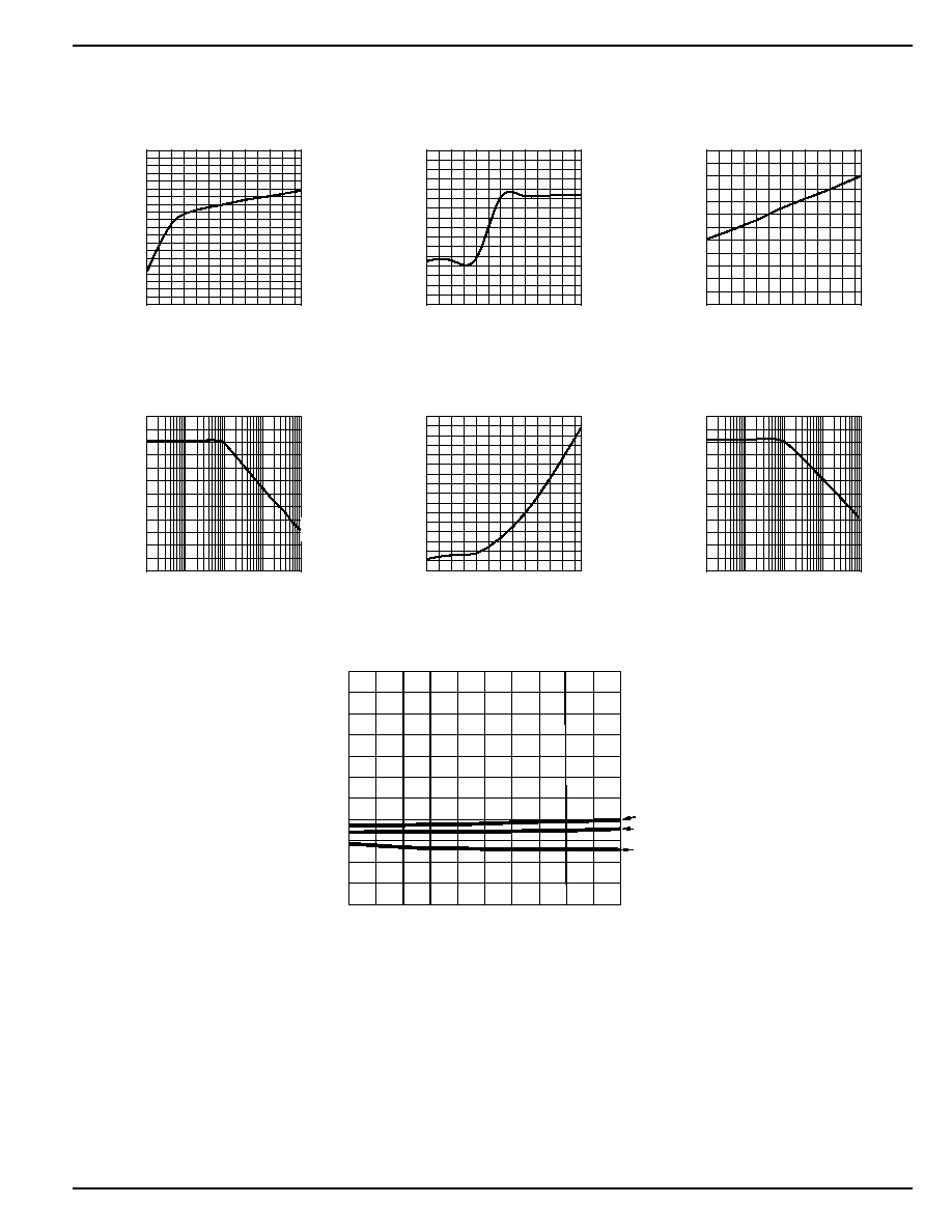
Closed Loop Frequency Response AV = 1
0
+5
+10
+15
≠5
≠10
≠15
10k
0.1
µ
F
0.01
µ
F
1000pF
470pF
100pF
3pF
100k
1M
10M
1k
FREQUENCY (Hz)
Closed Loop Gain (A
V
= +1)
vs. Load Capacitance
GAIN (dB)
Functional Characteristics
≠20
≠10
0
+10
+20
≠30
≠40
≠50
10k
100k
1M
0
≠90
≠180
1k
100
10M
FREQUENCY (Hz)
GAIN (dB)
PHASE (
∞
)
Gain Bandwidth of MIC820

December 2000
5
MIC820
MIC820
Micrel
Applications Information
Power Supply Bypassing
Regular supply bypassing techniques are recommended. A
10
µ
F capacitor in parallel with a 0.1
µ
F capacitor on both the
positive and negative supplies are ideal. For best perfor-
mance all bypassing capacitors should be located as close to
the op amp as possible and all capacitors should be low ESL
(equivalent series inductance), ESR (equivalent series resis-
tance). Surface-mount ceramic capacitors are ideal.