January 2000
1
MIC833
MIC833
Micrel
MIC833
Comparator and Reference with Adj. Hystersis
Advance Information
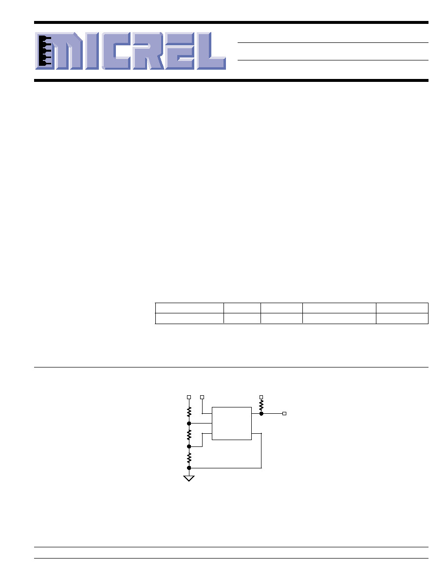
Typical Application
HTH
OUT
VDD
LTH
GND
MIC833
R
PU
V
IN
R1
R2
R3
V
OUT
V
DD
V
PULL-UP
V
LTH
> V
HTH
V
REF
= 1.24V
V
LTH(max)
= V
HTH(max)
= 6V
V
PULL-UP(max)
= 6V
1.5V
V
DD
5.5V
5
3
1
4
2
Features
� Optimized for PDAs, cellular telephones, pagers,
and other battery-powered devices
� Inputs and output can pulled up to 6V
regardless of supply voltage
� Independently adjustable high- and
low-voltage thresholds
� High
�
1% voltage threshold accuracy
� Extremely low 1
�
A typical supply current
� Immune to brief input transients
� 5-lead SOT-23 package
Applications
� PDAs
� Pagers
� Cordless phones
� Consumer electronics
� Embedded controllers
� Personal electronics
Micrel, Inc. � 1849 Fortune Drive � San Jose, CA 95131 � USA � tel + 1 (408) 944-0800 � fax + 1 (408) 944-0970 � http://www.micrel.com
General Description
The MIC833 is a micropower precision dual voltage com-
parator with an on-chip reference and latch.
High- and low-voltage thresholds are adjusted indepen-
dently, allowing for wide hysteresis. Three external resistors
determine the threshold voltages. Voltage detection thresh-
olds are accurate to 1%.
Supply current is extremely low (1
�
A, typical), making it ideal
for portable applications.
The MIC833 is supplied in Micrel's IttyBittyTM 5-lead SOT-23-
5 package.
See the MIC2778 for applications requiring an output delay.
IttyBittyTM is a trademark of Micrel, Inc.
Ordering Information
Part Number
Marking
Accuracy
Temperature Range
Package
MIC833BM5
B11
1%
�40
�
C to +85
�
C
SOT-23-5
MIC833
Micrel
MIC833
2
January 2000
Pin Description
Pin Number
Pin Name
Pin Function
1
HTH
High-Voltage Threshold (Input): Analog input to a comparator. This is the
voltage input assigned to detect a high-voltage condition when the level on
this pin exceeds V
REF
, OUT is asserted and the condition is latched until
V
LTH
< V
REF
.
2
GND
Ground
3
LTH
Low-Voltage Threshold (Input): Analog input to a comparator. This is the
voltage input assigned to detect a low voltage condition. When the level on
this pin falls below V
REF
, OUT is de-asserted and the condition is latched
until V
HTH
> V
REF
.
4
OUT
Output: Active-high, open-drain output. This output is de-asserted and
latched when V
LTH
<V
REF
, indicating a low voltage condition. This state
remains latched until V
HTH
> V
REF
.
5
VDD
Power Supply (Input): Independent supply input for internal circuitry.
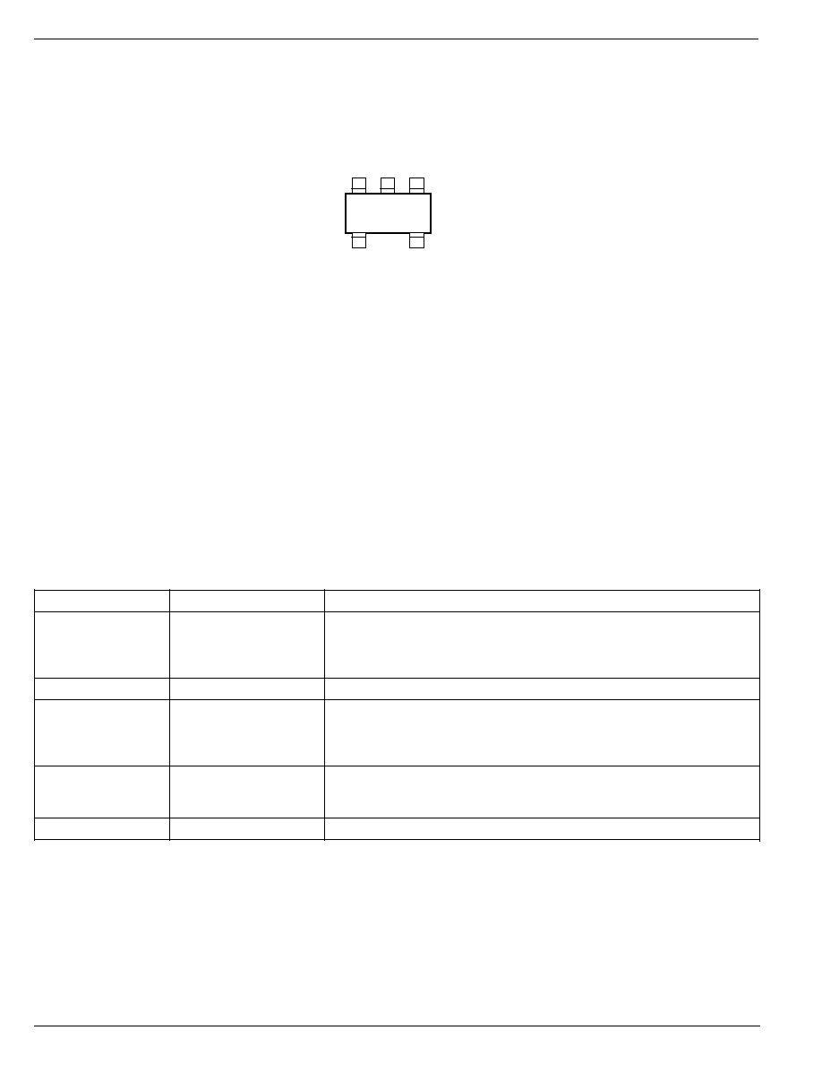
Pin Configuration
HTH
VDD
OUT
LTH
1
3
4
5
2
GND
SOT-23-5 (M5)
January 2000
3
MIC833
MIC833
Micrel
Absolute Maximum Ratings
(Note 1)
Supply Voltage (V
DD
) ..................................... �0.3V to +7V
Input Voltages (V
LTH
, V
HTH
) .......................................... +7V
Output Current (I
OUT
) ................................................. 20mA
Storage Temperature (T
S
) ....................... �65
�
C to +150
�
C
ESD Rating, Note 3 ...................................................... 2kV
Operating Ratings
(Note 2)
Supply Voltage (V
DD
) .................................. +1.5V to +5.5V
Input Voltage (V
LTH
, V
HTH
) ............................ �0.3V to +6V
Ambient Temperature Range (T
A
) ............. �40
�
C to +85
�
C
Junction Temperature (T
J
) ....................... Internally Limited
Package Thermal Resistance (
JA
) ...................... 260
�
C/W
Electrical Characteristics
1.5V
V
DD
5.5V; T
A
= +25
�
C, bold values indicate �40
�
C
T
A
+85
�
C; unless noted
Symbol
Parameter
Condition
Min
Typ
Max
Units
I
DD
Supply Current
outputs not asserted
1
2
�
A
I
LTH,
I
HTH
Input Leakage Current
0.005
10
nA
V
REF
Reference Voltage
1.228
1.240
1.252
V
t
D
Propagation Delay
V
LTH
= 1.352V to 1.128V
5
�
s
V
HTH
= 1.128V to 1.352V
5
�
s
V
OUT
Output Voltage-Low, Note 4
OUT de-asserted, I
SINK
= 1.6mA, V
DD
1.6V
0.3
V
OUT de-asserted, I
SINK
= 100
�
A, V
DD
1.2V
0.4
V
Note 1.
Exceeding the absolute maximum rating may damage the device.
Note 2.
The device is not guaranteed to function outside its operating rating.
Note 3.
Devices are ESD sensitive. Handling precautions recommended. Human body model, 1.5k in series with 100pF.
Note 4.
V
DD
operating range is 1.5V to 5.5V. output is guaranteed to be held low down to V
DD
= 1.2V.
Functional Diagram
V
HI
V
LO
V
IN
(Note B)
V
PULL-UP
0V
Note A
Note A
V
OUT
Note A.
Brief transients are ignored by the MIC833. See "Applications Information."
Note B.
V
LTH
> V
LO
>V
REF
.
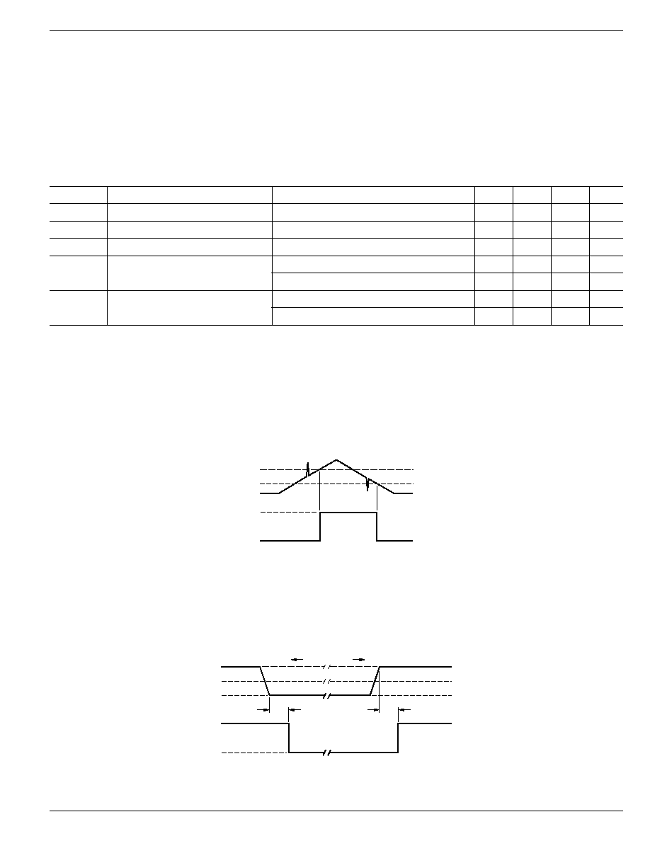
Timing Diagram
V
REF
+ 100mV
V
REF
� 100mV
V
REF
Inputs
V
PULL-UP
V
LTH
V
HTH
0V
t
D
t
D
V
OUT

MIC833
Micrel
MIC833
4
January 2000
Functional Description
The MIC833 monitors a voltage and detects when it is below
or above two independently programmed levels.
Voltage Low Output
The output (OUT) is an active-high, open-drain output which
sinks current when the MIC833 detects a low input voltage at
its LTH input. This condition is latched until the HTH input is
presented with a voltage higher than the internal V
REF
(+1.24V).
Block Diagram
GND
V
DD
+1.5V to +5.5V
OUT
1.24V
Bandgap
Reference
Low-Voltage
Detect
High-Voltage
Detect
R
S
Q
Q
LTH
HTH
V
LTH
V
HTH
MIC833
VDD
V
IN
3
1
2
4
5
Trip Points
Input voltage is monitored by the comparators via a voltage
divider network. The divided voltage is compared to an
internal reference voltage. When the voltage at the LTH input
pin drops below the internal reference voltage, the output
pulls low. Because of the voltage divider, the voltage at HTH
is assured to be below the reference voltage.

January 2000
5
MIC833
MIC833
Micrel
drain to 3.1V. Using 3.1V for the V
IN(lo)
threshold allows
calculation of the two remaining resistor values.
V
3.1V
1.24
1M
R2
344k
IN(lo)
=
=
+
R2
56k
=
1M
R2 R3
R1
-
-
(
)
=
R1 600k
=
The accuracy of the resistors can be chosen based upon the
accuracy required by the system.
The inputs may be subjected to voltages as high as 6V steady
state without adverse effects of any kind, regardless of the IC
supply voltage. This applys even if the supply voltage is zero.
This permits the situation in which the IC supply is turned off,
but voltage is still present on the inputs. See "Electrical
Characteritics."
Input Transients
The MIC833 is inherently immune to very short negative-
going "glitches." Very brief transients may exceed the V
IN(lo)
threshold without tripping the output.
As shown in Figure 2, the narrower the transient, the deeper
the threshold overdrive that will be ignored by the MIC833.
The graph represents the typical allowable transient duration
for a given amount of threshold overdrive that will not toggle
the output.
0
20
40
60
80
100
120
140
1
10
100
1000
MAX. TRANSIENT DURATION (
�
s)
RESET COMP. OVERDRIVE, V
REF
�V
LTH
(mV)
Input Transient
Response
Figure 2. Input Transient Response
Initialization Behavior
When the MIC833 is powered up, the comparators and latch
become active before the reference voltage reaches its final
value. In most applications, this presents no problems. How-
ever, the user should be aware of this: when applying power
to the part, if the input voltage is
between the two thresholds,
the output of the part will be
high because input HTH will have
been higher than the 1.24V reference during initialization.
It is not very likely the part would be powered up in this state;
it is more likely the same power supply will power the part and
develop its inputs. However, if the above-described condition
should occur, the next HTH threshold crossing would
not be
processed; that is, the latch would have been already set. The
next valid input condition would have to be a crossing of the
LTH threshold, which resets the latch, after which "normal"
operation is restored.
Applications Information
Output
Since the MIC833 output is an open-drain MOSFET, most
applications will require a pull-up resistor. The value of the
resistor should not be too large or leakage effects may
dominate. 470k
is the maximum recommended value. Note
that the output may be pulled up as high as 6V regardless of
IC supply voltage. See "Electrical Characteristics."
Programming the Thresholds
The low-voltage threshold is calculated using:
V
V
R1 R2 R3
R2 R3
IN(lo)
REF
=
+
+
+
The high-voltage threshold is calculated using:
V
V
R1 R2 R3
R3
IN(hi)
REF
=
+
+
where, for both equations:
V
1.240V
REF
=
In order to provide the additional criteria needed to solve for
the resistor values, the resistors can be selected such that
they have a given total value, that is, R1 + R2 + R3 = R
TOTAL
.
A value such as 1M
for R
TOTAL
is a reasonable value
because it draws minimum current but has no significant
effect on accuracy.
When working with large resistors, a small amount of leakage
current can cause voltage offsets that degrade system accu-
racy. The maximum recommended total resistance from V
IN
to ground is 3M
.
HTH
OUT
VDD
LTH
GND
MIC833
604k
1%
56k
1%
340k
1%
470k
V
IN
R1
R2
R3
V
OUT
V
DD
5
3
1
4
2
Figure 1. Example Circuit
Once the desired trip points are determined, set the V
IN(hi)
threshold first.
For example, use a total of 1M
= R1 + R2 + R3. For a typical
single-cell lithium ion battery, 3.6V is a good "high threshold"
because at 3.6V the battery is moderately charged. Solving
for R3:
V
3.6V
1.24
1M
R3
IN(hi)
=
=
R3
344k
=
Once R3 is determined, the equation for V
IN(lo)
can be used
to determine R2. A single lithium-ion cell, for example, should
not be discharged below 2.5V. Many applications limit the