 | –≠–ª–µ–∫—Ç—Ä–æ–Ω–Ω—ã–π –∫–æ–º–ø–æ–Ω–µ–Ω—Ç: MIC863BM8 | –°–∫–∞—á–∞—Ç—å:  PDF PDF  ZIP ZIP |

January 2005
1
MIC863
MIC863
Micrel
MIC863
Dual Ultra Low Power Op Amp in SOT23-8
Final Information
General Description
The MIC863 is a dual low power operational amplifier in
SOT23-8 package. It is designed to operate in the 2V to 5V
range, rail-to-rail output, with input common-mode to ground.
The MIC863 provides 450kHz gain-bandwidth product while
consuming only a 4.2µA supply current.
With low supply voltage and SOT23-8 packaging, MIC863
provides two channels as general-purpose amplifiers for
portable and battery-powered applications. Its package pro-
vides the maximum performance available while maintaining
an extremely slim form factor. The minimal power consump-
tion of this IC maximizes the battery life potential.
Typical Application
50
0.1µF
10µF
100pF
510
1
/
2
MIC863
1
/
2
MIC863
V
OUT
V+
RF
Peak Detector Circuit for AM Radio
Features
∑ SOT23-8 packaging
∑ 450kHz gain-bandwidth product
∑ 800kHz, ≠3dB bandwidth
∑ 4.2µA supply current/channel
∑ Rail-to-rail output
∑ Ground sensing at input (common mode to GND)
∑ Drives large capactive loads (0.02µF)
∑ Unity gain stable
Applications
∑ Portable equipment
∑ Medical instrument
∑ PDAs
∑ Pagers
∑ Cordless phones
∑ Consumer electronics
Micrel, Inc. ∑ 1849 Fortune Drive ∑ San Jose, CA 95131 ∑ USA ∑ tel + 1 (408) 944-0800 ∑ fax + 1 (408) 944-0970 ∑ http://www.micrel.com
Ordering Information
Part Number
Standard
Marking
Pb-Free
Marking
Ambient Temp. Range
Package
MIC863BM8
A35
MIC863YM8
A35
≠40∞C to +85∞C
SOT23-8
MIC863
Micrel
MIC863
2
January 2005
Pin Description
Pin Number
Pin Name
Pin Function
1
OUTA
Output: Amplifier A Output
2
INA≠
Amplifier A Inverting (Input)
3
INA+
Amplifier A Non-Inverting (Input)
4
V≠
Negative Supply
5
INB+
Amplifier B Non-Inverting (Input)
6
INB≠
Amplifier B Inverting (Input)
7
OUTB
Output: Amplifier B Output
8
V+
Positive Supply
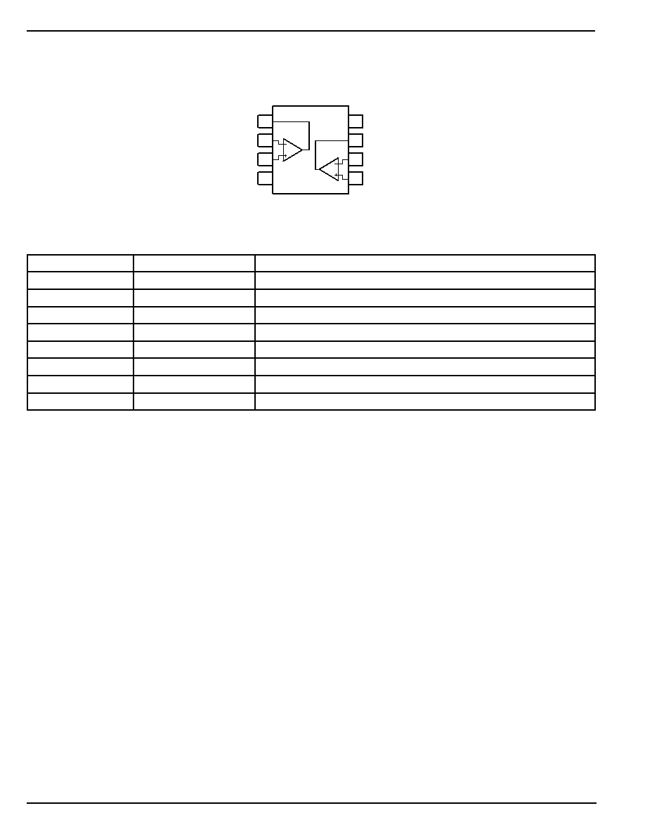
Pin Configuration
1
OUTA
INA≠
INA+
V≠
8
V+
OUTB
INB≠
INB+
7
6
5
2
3
4
SOT23-8 (M8)
January 2005
3
MIC863
MIC863
Micrel
Absolute Maximum Ratings
(Note 1)
Supply Voltage (V
V+
≠ V≠) ......................................... +6.0V
Differential Input Voltage (V
IN+
≠ V
IN≠
), Note 4 ...... +6.0V
Input Voltage (V
IN+
≠ V
IN≠
) .................. V
+
+ 0.3V, V
≠
≠0.3V
Lead Temperature (soldering, 5 sec.) ....................... 260∞C
Output Short Circuit Current Duration .................. Indefinite
Storage Temperature (T
S
) ........................................ 150∞C
ESD Rating, Note 3
Operating Ratings
(Note 2)
Supply Voltage (V+ ≠ V≠) .......................... +2.0V to +5.25V
Ambient Temperature Range ..................... ≠40∞C to +85∞C
Package Thermal Resistance
JA
(Using 4 layer PCB) ................................. 100∞C/W
CA
(Using 4 layer PCB) ................................... 70∞C/W
Electrical Characteristics
V+ = +2V, V≠ = 0V, V
CM
= V+/2; R
L
= 500k to V+/2; T
A
= 25∞C, unless otherwise noted. Bold values indicate ≠40∞C T
A
+85∞C.
Symbol
Parameter
Condition
Min
Typ
Max
Units
V
OS
Input Offset Voltage
≠6
0.1
6
mV
≠5
5
Differential Offset Voltage
0.5
mV
Input Offset Voltage Temp Coefficient
6
µV/∞C
I
B
Input Bias Current
10
pA
I
OS
Input Offset Current
5
pA
V
CM
Input Voltage Range
CMRR > 50dB
0.5
1
V
CMRR
Common-Mode Rejection Ratio
0 < V
CM
< 1V
45
75
dB
PSRR
Power Supply Rejection Ratio
Supply voltage change of 2V to 2.7V
50
85
dB
A
VOL
Large-Signal Voltage Gain
R
L
= 100k, V
OUT
1.4V
PP
66
81
dB
R
L
= 500k, V
OUT
1.4V
PP
73
90
dB
V
OUT
Maximum Output Voltage Swing
R
L
= 500k
V+≠3mV V+≠1.4mV
V
V
OUT
Minimum Output Voltage Swing
R
L
= 500k
V≠+0.5mV V≠+ 3mV
V
GBW
Gain-Bandwidth Product
R
L
= 200k, C
L
= 2pF, Av = 11
320
kHz
PM
Phase Margin
R
L
= 200k, C
L
= 2pF, Av = 11
69
∞
BW
≠3dB Bandwidth
A
V
= 1, C
L
= 2pF, R
L
= 1M
600
kHz
SR
Slew Rate
A
V
= 1, C
L
= 2pF, R
L
= 1M,
0.33
V/µs
Positive Slew Rate = 0.17V/µs
I
SC
Short-Circuit Output Current
Source
1.8
2.6
mA
Sink
1.5
2.2
mA
I
S
Supply Current (per Op Amp)
No Load
3.5
7
µA
Channel to Channel Crosstalk
Note 5
-100
dB
V+ = +2.7V, V≠ = 0V, V
CM
= V+/2; R
L
= 500k to V+/2; T
A
= 25∞C, unless otherwise noted. Bold values indicate ≠40∞C T
A
+85∞C.
V
OS
Input Offset Voltage
≠6
0.1
6
mV
≠5
5
Differential Offset Voltage
0.5
mV
Input Offset Voltage Temp Coefficient
6
µV/∞C
I
B
Input Bias Current
10
pA
I
OS
Input Offset Current
5
pA
V
CM
Input Voltage Range
CMRR > 60dB
1
1.8
V
CMRR
Common-Mode Rejection Ratio
0 < V
CM
< 1.35V
60
83
dB
PSRR
Power Supply Rejection Ratio
Supply voltage change from 2.7V to 3V
55
85
dB
A
VOL
Large-Signal Voltage Gain
R
L
= 100k, V
OUT
2V
PP
70
83
dB
R
L
= 500k, V
OUT
2V
PP
78
91
dB
MIC863
Micrel
MIC863
4
January 2005
Symbol
Parameter
Condition
Min
Typ
Max
Units
GBW
Gain-Bandwidth Product
R
L
= 200k, C
L
= 2pF, Av = 11
350
kHz
PM
Phase Margin
R
L
= 200k, C
L
= 2pF, Av = 11
65
∞
BW
≠3dB Bandwidth
A
V
= 1, C
L
= 2pF, R
L
= 1M
600
kHz
SR
Slew Rate
A
V
= 1, C
L
= 2pF, R
L
= 1M
0.35
V/µs
Positive Slew Rate = 0.17V/µs
I
SC
Short-Circuit Output Current
Source
4.5
6.3
mA
Sink
4.5
6.2
mA
I
S
Supply Current (per Op Amp)
No Load
3.6
7
µA
Channel to Channel Crosstalk
Note 5
≠120
dB
V+= +5V, V≠= 0V, V
CM
= V+/2; R
L
= 500k to V+/2; T
A
= 25∞C, unless otherwise noted. Bold values indicate ≠40∞C T
A
+85∞C.
V
OS
Input Offset Voltage
≠6
0.1
6
mV
≠5
5
Differential Offset Voltage
0.5
mV
Input Offset Voltage Temp Coefficient
6
µV/∞C
I
B
Input Bias Current
10
pA
I
OS
Input Offset Current
5
pA
V
CM
Input Voltage Range (from V≠)
CMRR > 60dB
3.5
4.1
V
CMRR
Common-Mode Rejection Ratio
0 < V
CM
< 3.5V
60
85
dB
PSRR
Power Supply Rejection Ratio
Supply voltage change from 3V to 5V
60
86
dB
A
VOL
Large-Signal Voltage Gain
R
L
= 100k, V
OUT
4.0V
PP
73
81
dB
R
L
= 500k, V
OUT
4.0V
PP
78
88
dB
V
OUT
Maximum Output Voltage Swing
R
L
= 500k
V+≠3mV V+≠1.3mV
V
V
OUT
Minimum Output Voltage Swing
R
L
= 500k
V≠+0.7mV V≠+3mV
V
GBW
Gain-Bandwidth Product
R
L
= 200k, C
L
= 2pF, Av = 11
450
kHz
PM
Phase Margin
63
∞
BW
≠3dB Bandwidth
A
V
= 1, C
L
= 2pF, R
L
= 1M
800
kHz
SR
Slew Rate
A
V
= 1, C
L
= 2pF, R
L
= 1M
0.35
V/µs
Positive Slew Rate = 0.2V/µs
I
SC
Short-Circuit Output Current
Source
17
23
mA
Sink
18
27
mA
I
S
Supply Current (per Op Amp)
No Load
4.2
8
µA
Channel to Channel Crosstalk
Note 5
≠120
dB
Note 1.
Exceeding the absolute maximum rating may damage the device.
Note 2.
The device is not guaranteed to function outside its operating rating.
Note 3.
Devices are ESD sensitive. Handling precautions recommended. Human body model, 1.5k in series with 100pF. Pin 4 is ESD sensitive
Note 4.
Exceeding the maximum differential input voltage will damage the input stage and degrade performance (in particular, input bias current is
likely to increase.
Note 5.
DC signal referenced to input. Refer to Typical Characteristics graphs for AC performance.
January 2005
5
MIC863
MIC863
Micrel
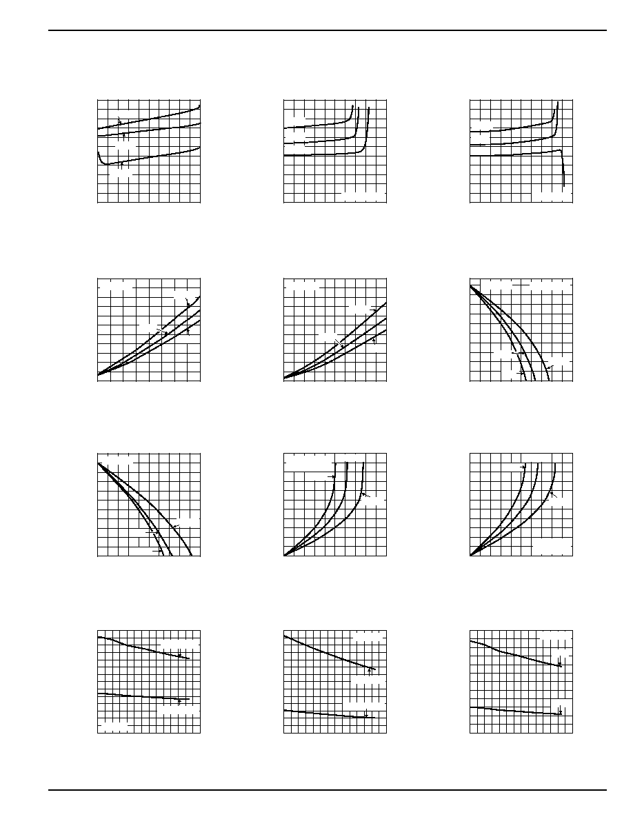
DC Performance Characteristics
0
5
10
15
20
25
30
35
-40 -20
0
20
40
60
80 100
SHORT CIRCUIT CURRENT (mA)
TEMPERATURE (∞C)
Short Circuit Current
vs. Temperature
V± = 2.5V
V± = ±1.35V
Sinking
0
5
10
15
20
25
30
-40 -20
0
20
40
60
80 100
SHORT CIRCUIT CURRENT (mA)
TEMPERATURE (∞C)
Short Circuit Current
vs. Temperature
1.35V
2.5V
Sourcing
1.0
1.4
1.8
2.2
2.6
3.0
3.4
3.8
4.2
4.6
5.0
5.4
0.90
1.06
1.22
1.38
1.54
1.70
1.86
2.02
2.18
2.34
2.50
SUPPLY CURRENT (
µ
A)
SUPPLY VOLTAGE (V)
Supply Current
vs. Supply Voltage
25∞C
-45∞C
85∞C
-1.0
-0.8
-0.6
-0.4
-0.2
0
0.2
0.4
0.6
0.8
1.0
1.2
-1.35
-1.08
-0.81
-0.54
-0.27
0
0.27
0.54
0.81
1.08
1.35
OFFSET VOLTAGE (mV)
COMMON-MODE VOLTAGE (V)
Offset Voltage
vs. Common-Mode Voltage
-40∞C
85∞C
25∞C
V± = ±1.35V
-1.0
-0.8
-0.6
-0.4
-0.2
0
0.2
0.4
0.6
0.8
1.0
1.2
-2.5 -2 -1.5 -1 -0.5 0 0.5 1 1.5 2 2.5
OFFSET VOLTAGE (mV)
COMMON-MODE VOLTAGE (V)
Offset Voltage
vs. Common-Mode Voltage
85∞C
25∞C
-40∞C
V± = ±2.5V
0
3
6
9
12
15
18
21
24
27
30
33
0.9 1.1 1.3 1.5 1.7 1.9 2.1 2.3 2.5
SHORT-CIRCUIT CURRENT (mA)
SUPPPLY VOLTAGE (V)
Short Circuit Current
vs. Supply Voltage
85∞C
25∞C
-40∞C
Sourcing
0
4
8
12
16
20
24
28
32
36
40
44
0.9
1.06
1.22
1.38
1.54
1.7
1.86
2.02
2.18
2.34
2.5
SHORT-CIRCUIT CURRENT (mA)
SUPPLY VOLTAGE (±V)
Short Circuit Current vs.
Supply Voltage
85∞C
25∞C
-40∞C
Sinking
0
0.135
0.27
0.405
0.54
0.675
0.81
0.945
1.08
1.215
1.35
0 -1 -2 -3 -4 -5 -6 -7 -8 -9 -10
OUTPUT VOLTAGE (V)
OUTPUT CURRENT (mA)
Output Voltage
vs. Output Current
85∞C
25∞C
-40∞C
Sourcing
V± = ±1.35V
0
0.25
0.50
0.75
1.00
1.25
1.50
1.75
2.00
2.25
2.50
2.75
0 -3 -6 -9 -12-15-18-21-24-27-30
OUTPUT VOLTAGE (V)
OUTPUT CURRENT (mA)
Output Voltage
vs. Output Current
85∞C
≠40∞C
25∞C
Sourcing
-1.350
-1.215
-1.080
-0.945
-0.810
-0.675
-0.540
-0.405
-0.270
-0.135
0
0.135
0
1
2
3
4
5
6
7
8
9 10
OUTPUT VOLTAGE (V)
OUTPTU CURRENT (mA)
Output Voltage
vs. Output Current
≠40∞C
85∞C
25∞C
Sinking
V± = ±1.35V
-2.5
-2.25
-2
-1.75
-1.5
-1.25
-1
-0.75
-0.5
-0.25
0
0.25
0
4
8 12 16 20 24 28 32 36 40
OUTPUT VOLTAGE (V)
OUTPUT CURRENT (mA)
Output Voltage
vs. Output Current
≠40∞C
85∞C
25∞C
Sinking
V± = ±2.5V
-6
-1
4
9
14
19
24
29
-40 -20
0
20
40
60
80 100
SHORT-CIRCUIT CURRENT (mA)
TEMPERATURE (∞C)
Short Circuit Current
vs. Temperature
V± = ±2.5V
V± = ±1.35V
Sinking