 | –≠–ª–µ–∫—Ç—Ä–æ–Ω–Ω—ã–π –∫–æ–º–ø–æ–Ω–µ–Ω—Ç: MIC919BC5 | –°–∫–∞—á–∞—Ç—å:  PDF PDF  ZIP ZIP |
October 2001
1
MIC919
MIC919
Micrel
MIC919
27MHz Low-Power SOT-23-5/SC-70 Op Amp
Final Information
General Description
The MIC919 is a high-speed operational amplifier with a gain-
bandwidth product of 27MHz. The part is unity gain stable. It
has a very low 360
µ
A supply current, and features the
IttyBittyTM SOT-23-5 package and SC-70 package.
Supply voltage range is from
±
2.5V to
±
9V, allowing the
MIC919 to be used in low-voltage circuits or applications
requiring large dynamic range.
The MIC919 is stable driving any capacitative load and
achieves excellent PSRR and CMRR, making it much easier
to use than most conventional high-speed devices. Low
supply voltage, low power consumption, and small packing
make the MIC919 ideal for portable equipment. The ability to
drive capacitative loads also makes it possible to drive long
coaxial cables.
Features
∑ 27MHz gain bandwidth product
∑ 360
µ
A supply current
∑ SOT-23-5 or SC-70 packages
∑ 1500V/
µ
s slew rate
∑ drives any capacitive load
∑ Unity gain stable
Applications
∑ Video
∑ Imaging
∑ Ultrasound
∑ Portable equipment
∑ Line drivers
Ordering Information
Part Number
Junction Temp.
Range Package
MIC919BM5
≠40C to +85C
SOT-23-5*
MIC919BC5
≠40C to +85C
SC-70
*Contact factory about SOT-23-5 package.
Micrel, Inc. ∑ 1849 Fortune Drive ∑ San Jose, CA 95131 ∑ USA ∑ tel + 1 (408) 944-0800 ∑ fax + 1 (408) 944-0970 ∑ http://www.micrel.com
Pin Description
Pin Number
Pin Name
Pin Function
1
IN+
Noninverting Input
2
V≠
Negative Supply (Input)
3
IN≠
Inverting Input
4
OUT
Output: Amplifier Output
5
V+
Positive Supply (Input)
Pin Configuration
IN+
V--
OUT
IN--
1
3
4
5
2
V+
A31
Part
Identification
SOT-23-5 or SC-70
Functional Pinout
IN+
V--
OUT
IN--
1
3
4
5
2
V+
SOT-23-5 or SC-70

MIC919
Micrel
MIC919
2
October 2001
Absolute Maximum Ratings
(Note 1)
Supply Voltage (V
V+
≠ V
V≠
) ........................................... 20V
Differentail Input Voltage (
V
IN+
≠ V
IN≠
) .......... 4V, Note 3
Input Common-Mode Range (V
IN+
, V
IN≠
) .......... V
V+
to V
V≠
Lead Temperature (soldering, 5 sec.) ....................... 260
∞
C
Storage Temperature (T
S
) ........................................ 150
∞
C
ESD Rating, Note 4 ................................................... 1.5kV
Operating Ratings
(Note 2)
Supply Voltage (V
S
) .......................................
±
2.5V to
±
9V
Junction Temperature (T
J
) ......................... ≠40
∞
C to +85
∞
C
Package Thermal Resistance
SOT-23-5 .......................................................... 260
∞
C/W
SC-70-5 ............................................................. 450
∞
C/W
Electrical Characteristics (
±
5V)
V+ = +5V, V≠ = ≠5V, V
CM
= 0V, R
L
= 10M
; T
J
= 25
∞
C, bold values indicate ≠40
∞
C
T
J
+85
∞
C; unless noted.
Symbol
Parameter
Condition
Min
Typ
Max
Units
V
OS
Input Offset Voltage
0.43
5
mV
V
OS
V
OS
Temperature Coefficient
1
µ
V/
∞
C
I
B
Input Bias Current
0.13
0.6
µ
A
I
OS
Input Offset Current
0.06
0.3
µ
A
V
CM
Input Common-Mode Range
CMRR > 72dB
≠3.25
+3.25
V
CMRR
Common-Mode Rejection Ratio
≠2.5V < V
CM
< +2.5V
75
87
dB
PSRR
Power Supply Rejection Ratio
±
3.5V < V
S
<
±
9V
95
105
dB
A
VOL
Large-Signal Voltage Gain
R
L
= 2k, V
OUT
=
±
2V
70
84
dB
R
L
= 100
, V
OUT
=
±
1V
85
dB
V
OUT
Maximum Output Voltage Swing
positive, R
L
= 2k
+3.0
3.7
V
negative, R
L
= 2k
≠3.7
≠3.0
V
positive, R
L
= 200
+1.5
3.0
V
negative, R
L
= 200
, Note 5
≠2.5
≠1.0
V
GBW
Unity Gain-Bandwidth Product
23
MHz
PM
Phase Margin
63
∞
BW
≠3dB Bandwidth
53
MHz
SR
Slew Rate
C=1.7pF, Gain=1, V
OUT
=5V, peak to peak,
850
V/
µ
s
positive SR = 450V/
µ
s
I
SC
Short-Circuit Output Current
source
45
57
mA
sink
20
40
mA
I
S
Supply Current
No Load
0.30
0.50
mA
Input Voltage Noise
f = 10kHz
10
nV/
Hz
Input Current Noise
f = 10kHz
0.78
pA/
Hz
Electrical Characteristics
V+ = +9V, V≠ = ≠9V, V
CM
= 0V, R
L
= 10M
; T
J
= 25
∞
C, bold values indicate ≠40
∞
C
T
J
+85
∞
C; unless noted
Symbol
Parameter
Condition
Min
Typ
Max
Units
V
OS
Input Offset Voltage
0.4
5
mV
V
OS
Input Offset Voltage
1
µ
V/
∞
C
Temperature Coefficient
I
B
Input Bias Current
0.13
0.60
µ
A
I
OS
Input Offset Current
0.06
0.3
µ
A
V
CM
Input Common-Mode Range
CMRR > 75dB
≠7.25
+7.25
V
CMRR
Common-Mode Rejection Ratio
≠6.5V < V
CM
< +6.5V
75
87
dB
PSRR
Power Supply Rejection Ratio
±
3.5V < V
S
<
±
9V
95
105
dB
October 2001
3
MIC919
MIC919
Micrel
Symbol
Parameter
Condition
Min
Typ
Max
Units
A
VOL
Large-Signal Voltage Gain
R
L
= 2k, V
OUT
=
±
2V
75
86
dB
R
L
= 100
, V
OUT
=
±
1V
92
dB
V
OUT
Maximum Output Voltage Swing
positive, R
L
= 2k
6.5
7.6
V
negative, R
L
= 2k
≠7.6
≠6.2
V
GBW
Unity Gain-Bandwidth Product
27
MHz
PM
Phase Margin
61
∞
BW
≠3dB Bandwidth
60
MHz
SR
Slew Rate
C=1.7pF, Gain=1, V
OUT
=5V, peak to peak,
1500
V/
µ
s
positive SR = 750V/
µ
s
I
SC
Short-Circuit Output Current
source
40
59
mA
sink
25
45
mA
I
S
Supply Current
No Load
0.36
0.6
mA
Input Voltage Noise
f = 10kHz
10
nV/
Hz
Input Current Noise
f = 10kHz
0.78
pA/
Hz
Note 1.
Exceeding the absolute maximum rating may damage the device.
Note 2.
The device is not guaranteed to function outside its operating rating.
Note 3.
Exceeding the maximum differential input voltage will damage the input stage and degrade performance (in particular, input bias current is
likely to change).
Note 4.
Devices are ESD sensitive. Handling precautions recommended. Human body model, 1.5k in series with 100pF.
Note 5.
Output swing limited by the maximum output sink capability.
MIC919
Micrel
MIC919
4
October 2001
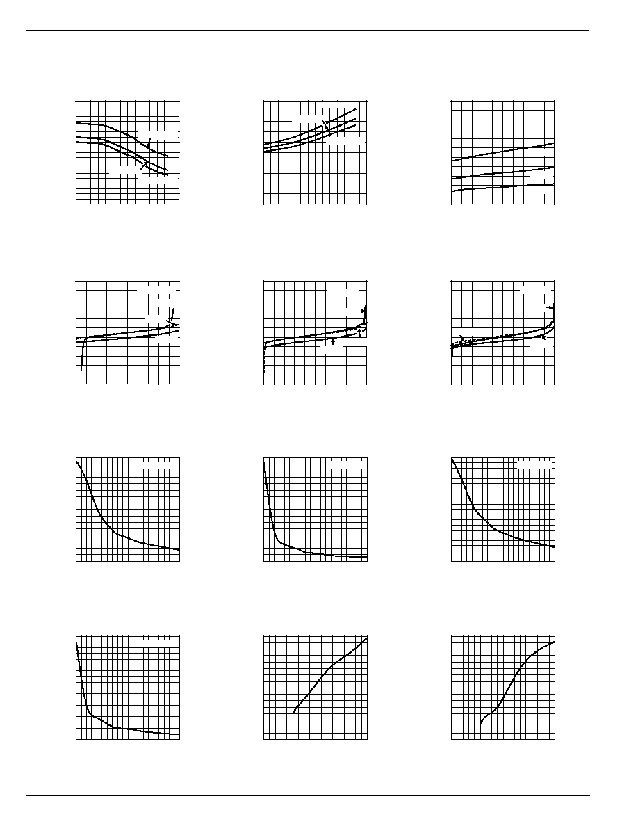
Typical Characteristics
0
100
200
300
400
500
600
700
800
0
100
200
300
400
500
600
700
800
900
1000
SLEW RATE (V/
µ
s)
LOAD CAPACITANCE (pF)
Positive Slew Rate vs.
Load Capacitance
V+ =
±
9V
0
200
400
600
800
1000
1200
1400
1600
0
100
200
300
400
500
600
700
800
900
1000
SLEW RATE (V/
µ
s)
LOAD CAPACITANCE (pF)
Negative Slew Rate vs.
Load Capacitance
V+ =
±
9V
0
50
100
150
200
250
300
350
400
450
500
0
100
200
300
400
500
600
700
800
900
1000
SLEW RATE (V/
µ
s)
LOAD CAPACITANCE (pF)
Positive Slew Rate vs.
Load Capacitance
V+ =
±
5V
0
100
200
300
400
500
600
700
800
900
0
100
200
300
400
500
600
700
800
900
1000
SLEW RATE (V/
µ
s)
LOAD CAPACITANCE (pF)
Negative Slew Rate vs.
Load Capacitance
V+ =
±
5V
0.5
0.55
0.6
0.65
0.7
0.75
0.8
0.85
0.9
0.95
1
-40 -20
0
20
40
60
80 100
OFFSET VOLTAGE (mV)
TEMPERATURE (
∞
C)
Offset Voltage
vs. Temperature
V
±
=
±
2.5V
V
±
=
±
5V
V
±
=
±
9V
0.10
0.15
0.20
0.25
0.30
0.35
-40 -20
0
20
40
60
80 100
SUPPLY CURRENT (mA)
TEMPERATURE (
∞
C)
Supply Current
vs. Temperature
V
±
=
±
2.5V
V
±
=
±
9V
V
±
=
±
5V
0.20
0.22
0.24
0.26
0.28
0.30
0.32
0.34
0.36
0.38
0.40
0.42
2.5
3.8
5.1
6.4
7.7
9
SUPPLY CURRENT (
µ
A)
SUPPLY VOLTAGE (V)
Supply Current
vs. Supply Voltage
≠40
∞
C
+85
∞
C
+25
∞
C
0
0.20
0.40
0.60
0.80
1.00
1.20
1.40
1.60
1.80
2.00
2.20
-900
-540
-180
180
540
900
OFFSET VOLTAGE (mV)
COMMON-MODE VOLTAGE (V)
Offset Voltage vs.
Common-Mode Voltage
≠40
∞
C
+85
∞
C
+25
∞
C
V
±
=
±
2.5V
0
0.2
0.4
0.6
0.8
1
1.2
1.4
1.6
1.8
2
2.2
-3.4
-2.7
-2.0
-1.4
-0.7
0.0
0.7
1.4
2.0
2.7
3
OFFSET VOLTAGE (mV)
COMMON-MODE VOLTAGE (V)
Offset Voltage vs.
Common-Mode Voltage
≠40
∞
C
+85
∞
C
+25
∞
C
V
±
=
±
5V
0
0.2
0.4
0.6
0.8
1
1.2
1.4
1.6
1.8
2
2.2
-7.40
-5.92
-4.44
-2.96
-1.48
0
1.48
2.96
4.44
5.92
7.40
OFFSET VOLTAGE (mV)
COMMON-MODE VOLTAGE (V)
Offset Voltage vs.
Common-Mode Voltage
≠40
∞
C
+85
∞
C
+25
∞
C
V
±
=
±
9V
0
100
200
300
400
500
600
700
800
0
1
2
3
4
5
6
7
8
9
POSITIVE SLEW RATE (V/
µ
s)
SUPPLY VOLTAGE (
±
V)
Positive Slew Rate
vs. Supply Voltage
0
200
400
600
800
1000
1200
1400
1600
0
1
2
3
4
5
6
7
8
9
NEGATIVE SLEW RATE (V/
µ
s)
SUPPLY VOLTAGE (
±
V)
Negative Slew Rate
vs. Supply Voltage
October 2001
5
MIC919
MIC919
Micrel
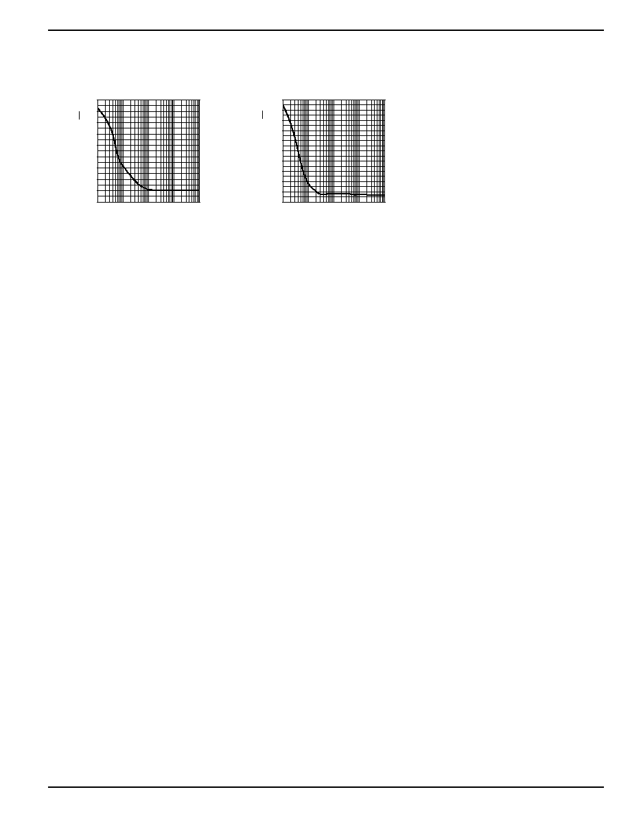
0
10
20
30
40
50
60
70
80
90
10
100
1000
10000 100000
NOISE VOLTAGE (nV/
Hz)
FREQUENCY (Hz)
Voltage Noise
0
0.5
1
1.5
2
2.5
3
3.5
4
4.5
5
10
100
1000
10000 100000
CURRENT NOISE (pA/
Hz)
FREQUENCY (Hz)
Current Noise