
August 1998
6-37
MIC94001
Micrel
6
MIC94001
P-Channel MOSFET
Not Recommended for New Designs
General Description
The MIC94001 is a silicon gate P-channel MOSFET de-
signed for low on-resistance, high-side switch applications.
The MIC94001 has a maximum on-resistance of 0.4
at 4.5V
gate-to-source voltage.
Improved ESD protection is provided by the gate protection
network shown in the schematic diagram.
The MIC94001 is supplied in a low-profile version of the
8-lead SOIC package.
The MIC94001 die can be assembled in a 4-terminal configu-
ration with the body not shorted to the source for use in analog
switch applications. Contact the factory for more information.
Features
∑ 15V minimum drain-to-source breakdown
∑ 0.4
maximum on-resistance at
4.5V gate-to-source
∑ Functional at 2.7V gate-to-source
∑ 0.063" maximum height
Applications
∑ High-side switch
∑ Power management
∑ Stepper motor control
∑ 1.8" PCMCIA disk-drive V
CC
switch
Ordering Information
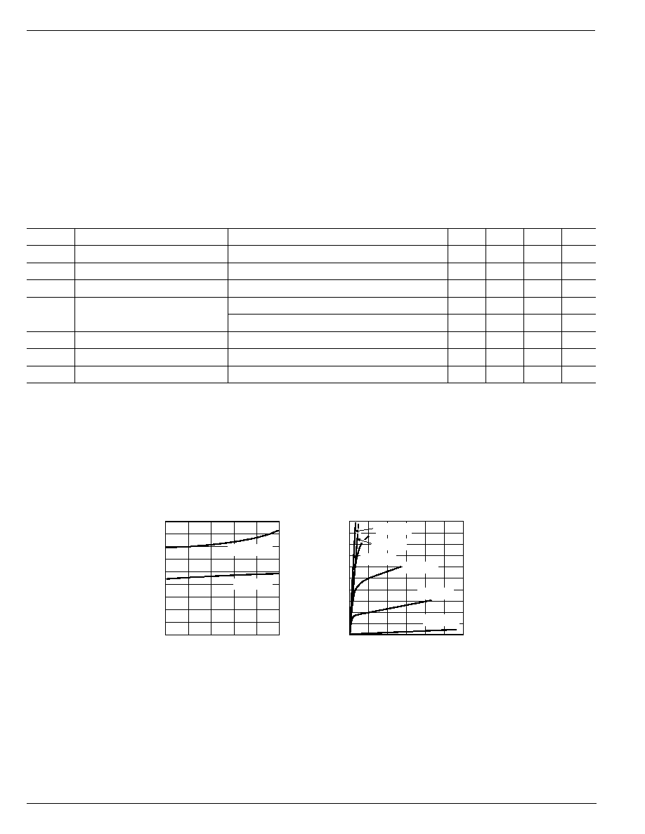
Part Number
Temperature Range*
Package
MIC94001BLM
≠55
∞
C to +150
∞
C
8-lead SOIC
* Operating Junction Temperature
Low Profile Leads, see Package Information
Package Information
Pin Configuration
1
2
3
4
8
7
6
5
Drain
Drain
Drain
Drain
NC
Source
Source
Gate
8-lead Low-Profile SOIC
Package (LM)
45
∞
3
∞
≠6
∞
0.244 (6.20)
0.228 (5.80)
0.197 (5.0)
0.189 (4.8)
0.063 (1.60) MAX
SEATING
PLANE
0.026 (0.65)
MAX
)
0.016 (0.40)
TYP
0.154 (3.90)
0.057 (1.45)
0.049 (1.25)
0.193 (4.90)
0.050 (1.27)
TYP
Pin 1
Typical Application
Schematic Information
Gate
Source
Drain
G
S
D
Schematic Symbol
Schematic Diagram
Load
+5V
74HC04
On
Off
MIC94001
Power Switch Application
Patent 5,355,008
MIC94001
Micrel
6-38
August 1998
Electrical Characteristics
T
A
= 25
∞
C unless noted.
All values are negative. Signs not shown for clarity.
Symbol
Parameter
Condition
Min
Typ
Max
Units
V
BDSS
Drain-Source Breakdown Voltage
V
GS
= 0V, I
D
= 250
µ
A
15
V
V
GS
Gate Threshold Voltage
V
DS
= V
GS
, I
D
= 250
µ
A
1
3
V
I
GSS
Gate-Body Leakage
V
DS
= 0V, V
GS
= 15V, Note 2
100
nA
I
DSS
Zero Gate Voltage Drain Current
V
DS
= 15V, V
GS
= 0V
25
µ
A
V
DS
= 15V, V
GS
= 0V, T
J
= 125
∞
C
250
µ
A
I
D(ON)
On-State Drain Current
V
DS
10V, V
GS
= 10V, Note 1
5.5
A
R
DS(ON)
Drain-Source On-State Resist.
V
GS
= 4.5V, I
D
= 50mA
0.35
0.40
g
FS
Forward Transconductance
V
DS
= 15V, I
D
= 1A, Note 1
0.7
S
Note 1: Pulse Test: Pulse Width
300
µ
sec, Duty Cycle
2%
Note 2: ESD gate protection diode conducts during positive gate-to-source voltage excursions.
Absolute Maximum Ratings
Voltage and current values are negative. Signs not shown for clarity.
Drain-to-Source Voltage ................................................ 15V
Gate-to-Source Voltage ................................................ 15V
Continuous Drain Current
T
A
= 25
∞
C ................................................................. 1.6A
T
A
= 100
∞
C .................................................................. 1A
Operating Juction Temperature ................. ≠55
∞
C to +150
∞
Storage Temperature ............................... ≠55
∞
C to +150
∞
C
0.00
0.05
0.10
0.15
0.20
0.25
0.30
0.35
0.40
0.45
0.0
0.4
0.8
1.2
1.6
2.0
R
DS(ON)
(
)
I
D
(A)
On Resistance vs.
Drain Current
V
GS
= 4.5V
V
GS
= 10V
Note 1
Total Power Dissipation
T
A
= 25
∞
C ................................................................... 1W
T
A
= 100
∞
C .............................................................. 0.4W
Thermal Resistance
JA ......................................................................................
125
∞
C/W
JC ........................................................................................
76
∞
C/W
Lead Temperature
1/16" from case, 10s ........................................... +300
∞
C
0
200
400
600
800
1000
1200
1400
1600
1800
2000
0.0
2.5
5.0
7.5 10.0 12.5 15.0
I
D
(mA)
V
DS
(V)
Drain Characteristics
V
GS
= 4.0
V
GS
= 3.5
V
GS
= 3.0
V
GS
= 2.5
V
GS
= 2.0
V
GS
= 1.5
Note 1