July 2002
1
MIC94060/94061
MIC94060/94061
Micrel
MIC94060/94061
100m
SC-70-6 Smart Load Switch
Final
General Description
The MIC94060 and MIC94061 are smart high-side load
switches housed in the SC-70-6 package. The devices
contain a low on-resistance, 100m
(max) p-channel MOSFET
that is driven by built-in level-shift and slew-rate control
circuitry. The low on-resistance of the devices allows for them
to support over 2A of continuous current. The MIC94061
features an active pull-down circuit that discharges capaci-
tive loads through a 200
switch when the IC is set to the OFF
state.
Pull down circuitry keeps the MIC94060/1 in a default OFF
state until the EN pin is pulled to a high level. The built-in level
shift circuitry allows for a logic signal that may be different
from the supply voltage to switch the high-side P-channel
MOSFET on or off. The 1
µ
s turn-on slew rate control
prevents in-rush current from causing glitches on the supply
rail.
Battery life is saved in portable applications with the IC's low
quiescent current of 2
µ
A and low shutdown current of <1
µ
A.
Their 1.8V to 5.5V operating voltage range makes the
MIC94060/1 suitable for 1-cell Li Ion, 2- to 3-cell NiMH / NiCad
/ Alkaline, as well as other sub-5V input applications.
Integrating the level-shift and slew-rate control circuitry saves
valuable board space and reduces component placement
cost compared to discrete solutions.
The MIC94060/1 are housed in the
TeenyTM SC-70-6 pack-
age and have a junction temperature range of ≠40
∞
C to
+150
∞
C.
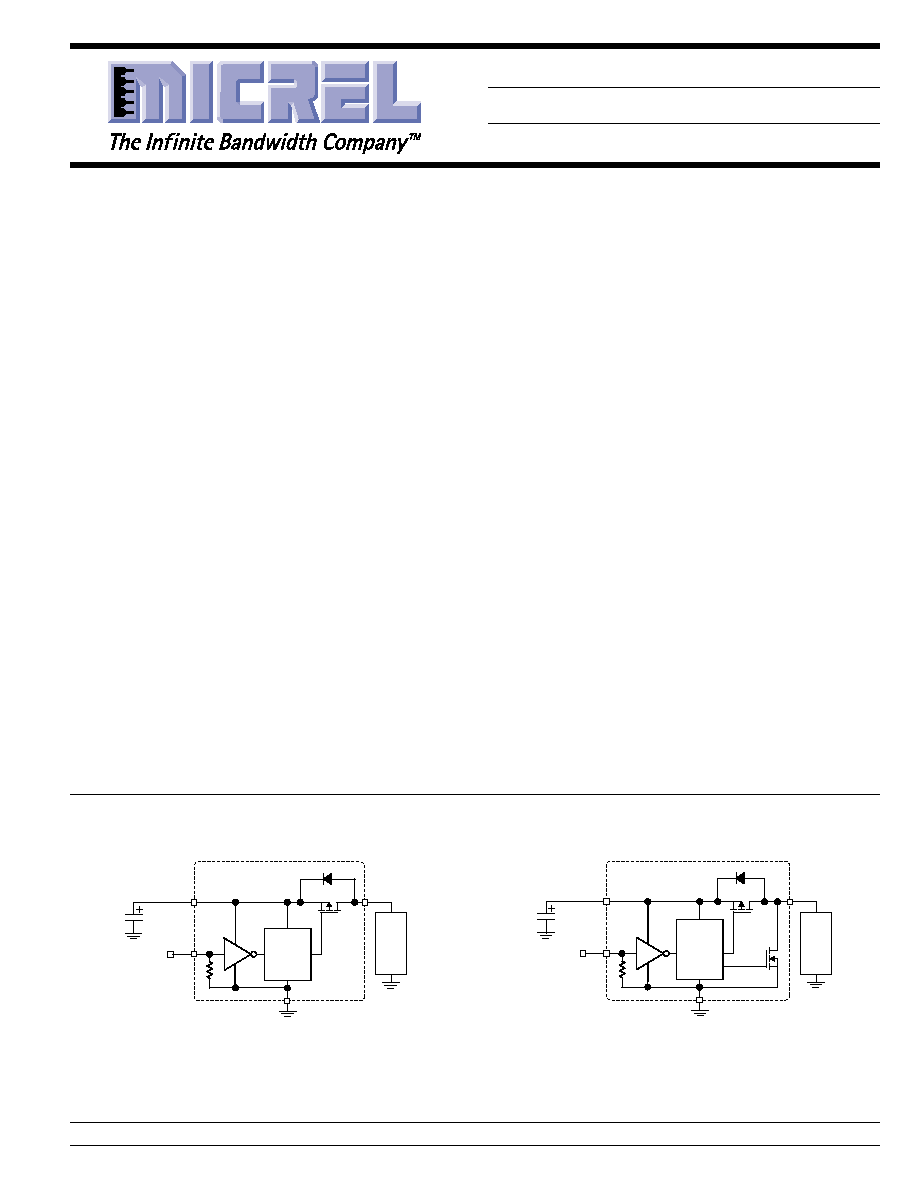
Typical Application
EN
V
IN
MIC94060
77m
9
LOAD
Level Shift
and
Slew Rate
Control
Load Switch Application
Features
∑ 1.8V to 5.5V input voltage range
∑ Built-in level shift circuitry:
Can be driven by 1.5V logic
∑ Low on-resistance p-channel MOSFET:
77m
at V
GS
= 4.5V (typ)
2A continuous current
∑ Built-in slew-rate control:
Controlled 1
µ
s turn-on rise-time
Fast 60ns turn-off fall time
∑ Low 2
µ
A quiescent current
∑ <1
µ
A micropower shutdown
∑ Built-in fast-off load discharge circuit (MIC94061)
∑
TeenyTM SC-70-6 package
∑ ≠40
∞
C to +150
∞
C junction temperature range
Applications
∑ Load switch in portable applications:
Cellular phones
PDAs
MP3 players
Digital cameras
Notebook PCs
Barcode scanners
∑ Battery switch over circuits
∑ Level translators
Micrel, Inc. ∑ 1849 Fortune Drive ∑ San Jose, CA 95131 ∑ USA ∑ tel + 1 (408) 944-0800 ∑ fax + 1 (408) 944-0970 ∑ http://www.micrel.com
EN
V
IN
MIC94061
77m
9
200
9
LOAD
Level Shift
Slew Rate
Control
and
Load
Discharge
Load Switch Application
with Capacitive Load Discharge
July 2002
3
MIC94060/94061
MIC94060/94061
Micrel
Absolute Maximum Ratings
(Note 1)
Input Voltage (V
IN
) ........................................................ +6V
Enable Voltage (V
EN
) .................................................... +6V
Continuous Drain Current (I
D
) Note 3
T
A
= 25
∞
C ..................................................................
±
2A
T
A
= 85
∞
C ...............................................................
±
1.4A
Pulsed Drain Current (I
DP
) Note 5 ................................
±
6A
Continuous Diode Current (I
S
) Note 7 ..................... ≠50mA
Power Dissipation Note 3
SC-70-6 lead (T
A
= 85
∞
C) .................................. 270 mW
Ambient Storage Temperature (T
S
) ......... ≠55
∞
C to +150
∞
C
ESD Rating Note 4
Operating Ratings
(Note 2)
Input Voltage Range (V
IN
) ............................... 1.8V to 5.5V
Junction Temperature Range (T
J
) ........... ≠40
∞
C to +150
∞
C
Package Thermal Impedance Note 3
JA
SC-70-6 lead ............................................... 240
∞
C/W
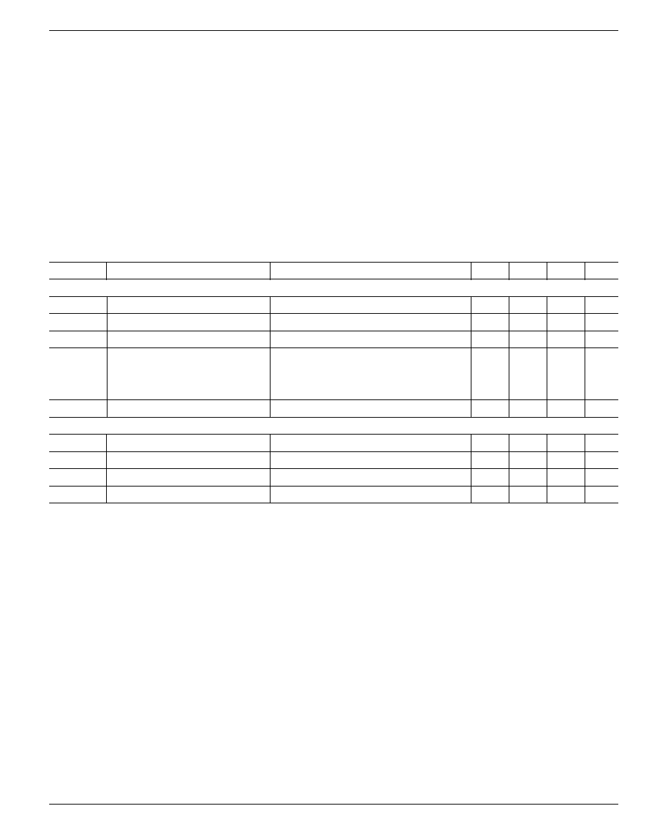
Electrical Characteristics
T
A
= 25
∞
C, unless otherwise specified.
Symbol
Parameter
Condition
Min
Typ
Max
Units
Static
V
EN(th)
EN Threshold Voltage
V
IN
= 1.8V to 4.5V, I
D
= ≠250
µ
A
0.5
1.2
V
I
EN
EN Input Current (Quiescent Current)
V
IN
= V
EN
= 5.5V
2
4
µ
A
I
VIN
OFF State Leakage Current
V
EN
= OPEN or 0V, V
IN
= +5.5V
1
µ
A
R
DS(ON)
P-Channel Drain-Source
V
IN
= 4.5V, I
D
= ≠100 mA; V
EN
= 1.5V
77
100
m
On-Resistance
V
IN
= 3.6V, I
D
= ≠100 mA; V
EN
= 1.5V
85
115
m
V
IN
= 2.5V, I
D
= ≠100 mA; V
EN
= 1.5V
100
140
m
V
IN
= 1.8V, I
D
= ≠100 mA; V
EN
= 1.5V
145
200
m
R
SHUTDOWN
Turn-off Impedance (94061)
V
IN
= 3.6V, V
EN
= 0V or OPEN
200
300
Dynamic (Note 6)
t
d(on)
Turn-On Delay Time
V
IN
= 3.6V, I
D
= ≠100mA, V
EN
= 1.5V
850
1500
ns
t
r
Turn-On Rise Time
V
IN
= 3.6V, I
D
= ≠100mA, V
EN
= 1.5V
0.5
1
5
µ
s
t
d(off)
Turn-Off Delay Time
V
IN
= 3.6V, I
D
= ≠100mA, V
EN
= 1.5V
100
150
ns
t
f
Turn-Off Fall Time
V
IN
= 3.6V, I
D
= ≠100mA, V
EN
= 1.5V
60
100
ns
Note 1.
T
A
= 25
∞
C unless otherwise noted. Absolute maximum ratings indicate limits beyond which damage to the component may occur. Electrical
specifications do not apply when operating the device outside of its operating ratings. The maximum allowable power dissipation is a function
of the maximum junction temperature, T
J(Max)
, the junction-to-ambient thermal resistance,
JA
, and the ambient temperature, T
A
.
Note 2.
This device is not guaranteed to operate beyond its specified operating rating.
Note 3.
Mounted on 1 square-inch pad of 2 oz. copper.
Note 4.
IC devices are inherently ESD sensitive. Handling precautions required.
Note 5.
Pulse width < 300
µ
s with <2% duty cycle.
Note 6.
Dynamic specifications are guaranteed by design.
Note 7.
Body diode current conduction is not recommended.