 | –≠–ª–µ–∫—Ç—Ä–æ–Ω–Ω—ã–π –∫–æ–º–ø–æ–Ω–µ–Ω—Ç: MICRF022 | –°–∫–∞—á–∞—Ç—å:  PDF PDF  ZIP ZIP |

March 2003
1
MICRF002/RF022
MICRF002/RF022
Micrel
MICRF002/RF022
300-440MHz QwikRadioTMASK Receiver
Final Information
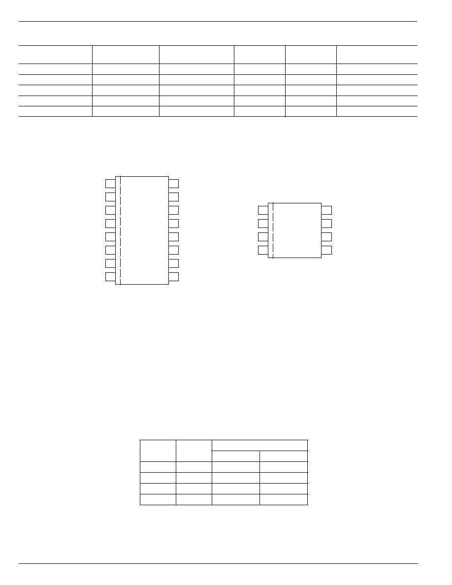
Typical Application
SEL0
SEL0
SWEN
VSSRF
REFOSC
VSSRF
SEL1
ANT
CAGC
VDDRF
WAKEB
VDDBB
SHUT
CTH
DO
NC
VSSBB
0.047uF
4.8970MHz
Data
Output
MICRF002
4.7uF
+5V
12nH
12pF
68nH
1/4 Wave Monopole
315MHz 800bps On-Off Keyed Receiver
Features
∑ 300MHz to 440MHz frequency range
∑ Data-rate up to 10kbps (fixed-mode)
∑ Low Power Consumption
∑ 2.2mA fully operational (315MHz)
∑ 0.9
µA in shutdown
∑ 220
µA in polled operation (10:1 duty-cycle)
∑ Wake-up output flag to enable decoders and micropro-
cessors
∑ Very low RF reradiation at the antenna
∑ Highly integrated with extremely low external part count
Applications
∑ Automotive Remote Keyless Entry (RKE)
∑ Remote controls
∑ Remote fan and light control
∑ Garage door and gate openers
Micrel, Inc. ∑ 1849 Fortune Drive ∑ San Jose, CA 95131 ∑ USA ∑ tel + 1 (408) 944-0800 ∑ fax + 1 (408) 944-0970 ∑ http://www.micrel.com
QwikRadio is a trademark of Micrel, Inc. The QwikRadio ICs were developed under a partnership agreement with AIT of Orlando, Florida.
General Description
The MICRF002 is a single chip ASK/OOK (ON-OFF Keyed)
RF receiver IC. This device is a true "antenna-in to data-out"
monolithic device. All RF and IF tuning is accomplished
automatically within the IC which eliminates manual tuning
and reduces production costs. The result is a highly reliable
yet low cost solution.
The MICRF002 is a fully featured part in 16-pin packaging,
the MICRF022 is the same part packaged in 8-pin packaging
with a reduced feature set (see "Ordering Information" for
more information).
The MICRF002 is an enhanced version of the MICRF001
and MICRF011. The MICRF002 provides two additional
functions over the MICRF001/011, (1) a Shutdown pin, which
may be used to turn the device off for duty-cycled operation,
and (2) a "Wake-up" output, which provides an output flag
indicating when an RF signal is present. These features make
the MICRF002 ideal for low and ultra-low power applications,
such as RKE and remote controls.
All IF filtering and post-detection (demodulator) data filtering
is provided within the MICRF002, so no external filters are
necessary. One of four demodulator filter bandwidths may be
selected externally by the user.
The MICRF002 offer two modes of operation; fixed-mode
(FIX) and sweep-mode (SWP). In fixed mode the MICRF002
functions as a conventional superhet receiver. In sweep
mode the MICRF002 employs a patented sweeping function
to sweep a wider RF spectrum. Fixed-mode provides better
selectivity and sensitivity performance and sweep mode
enables the MICRF002 to be used with low cost, imprecise
transmitters.
QwikRadioTM
MICRF002/RF022
Micrel
MICRF002/RF022
2
March 2003
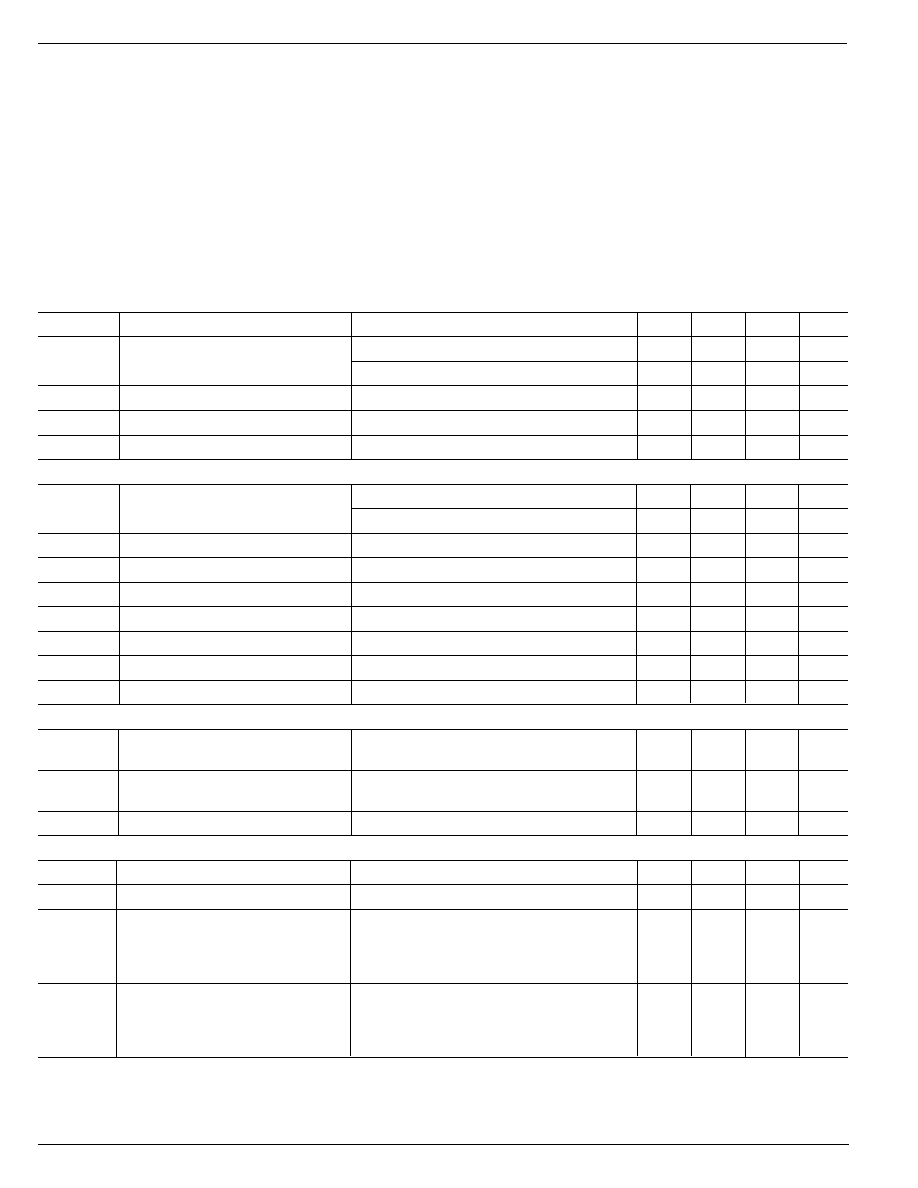
8-Pin Options
The standard 16-pin package allows complete control of all
configurable features. Some reduced function 8-pin versions
are also available, see "Ordering Information" above.
For high-volume applications additional customized 8-pin
devices can be produced. SWEN, SEL0 and SEL1 pins are
internally bonded to reduce the pin count. pin 6 may be
configured as either SHUT or WAKEB.
Pin Configuration
SEL0
SEL0
SWEN
VSSRF
REFOSC
VSSRF
SEL1
ANT
CAGC
VDDRF
WAKEB
VDDBB
SHUT
CTH
DO
NC
VSSBB
MICRF002Bx
1
16
2
15
3
14
4
13
5
12
6
11
7
10
8
9
VSSRF
REFOSC
ANT
CAGC
VDDRF
SHUT/WAKEB
CTH
DO
MICRF022Bx-xxxx
1
8
2
7
3
6
4
5
Standard 16-Pin or 8-Pin SOP (M) Packages
Ordering Information
Demodulator
WAKEB
Part Number
Bandwidth
Operating Mode
Shutdown
Output Flag
Package
MICRF002BM
User Programable
Fixed or Sweep
Yes
Yes
16-Pin SOP
MICRF022BM-SW48
5000Hz
Sweep
No
Yes
8-Pin SOP
MICRF022BM-FS12
1250Hz
Fixed
Yes
No
8-Pin SOP
MICRF022BM-FS24
2500Hz
Fixed
Yes
No
8-Pin SOP
MICRF022BM-FS48
5000Hz
Fixed
Yes
No
8-Pin SOP
0
L
E
S
1
L
E
S
h
t
d
i
w
d
n
a
B
r
o
t
a
l
u
d
o
m
e
D
e
d
o
M
p
e
e
w
S
e
d
o
M
D
E
X
I
F
1
1
z
H
0
0
0
5
z
H
0
0
0
0
1
0
1
z
H
0
0
5
2
z
H
0
0
0
5
1
0
z
H
0
5
2
1
z
H
0
0
5
2
0
0
z
H
5
2
6
z
H
0
5
2
1
Table 1. Nominal Demodulator Filter Bandwidth vs.
SEL0, SEL1 and Operating Mode

March 2003
3
MICRF002/RF022
MICRF002/RF022
Micrel
Pin Description
Pin Number
Pin Number
Pin Name
Pin Function
16-Pin Pkg.
8-Pin Pkg.
1
SEL0
Bandwidth Selection Bit 0 (Digital Input): Used in conjunction with SEL1 to
set the desired demodulator filter bandwidth. See Table 1. Internally pulled-
up to VDDRF
2, 3
1
VSSRF
RF Power Supply: Ground return to the RF section power supply.
4
2
ANT
Antenna (Analog Input): For optimal performance the ANT pin should be
impedance matched to the antenna. See "Applications Information" for
information on input impedance and matching techniques
5
3
VDDRF
RF Power Supply: Positive supply input for the RF section of the IC
6
VDDBB
Base-Band Power Supply: Positive supply input for the baseband section
(digital section) of the IC
7
4
CTH
Data Slicing Threshold Capacitor (Analog I/O): Capacitor connected to this
pin extracts the dc average value from the demodulated waveform which
becomes the reference for the internal data slicing comparator
8
NC
Not internally connected
9
VSSBB
Base-Band Power Supply: Ground return to the baseband section power
supply
10
5
DO
Data Output (Digital Output)
11
6
SHUT
Shutdown (Digital Input): Shutdown-mode logic-level control input. Pull low
to enable the receiver. Internally pulled-up to VDDRF
12
WAKEB
Wakeup (Digital Output): Active-low output that indicates detection of an
incoming RF signal
13
7
CAGC
Automatic Gain Control (Analog I/O): Connect an external capacitor to set
the attack/decay rate of the on-chip automatic gain control
14
SEL1
Bandwidth Selection Bit 1 (Digital Input): Used in conjunction with SEL0 to
set the desired demodulator filter bandwidth. See Table 1. Internally pulled-
up to VDDRF
15
8
REFOSC
Reference Oscillator: Timing reference, sets the RF receive frequency.
16
SWEN
Sweep-Mode Enable (Digital Input): Sweep- or Fixed-mode operation
control input. SWEN high= sweep mode; SWEN low = conventional
superheterodyne receiver. Internally pulled-up to VDDRF
MICRF002/RF022
Micrel
MICRF002/RF022
4
March 2003
Electrical Characteristics
V
DDRF
= V
DDBB
= V
DD
where +4.75V
V
DD
5.5V, V
SS
= 0V; C
AGC
= 4.7
µF, C
TH
= 100nF; SEL0 = SEL1 = V
SS
; fixed mode ( SWEN
= V
SS
); f
REFOSC
= 4.8970MHz (equivalent to f
RF
= 315MHz); data-rate = 1kbps (Manchester encoded). T
A
= 25
∞C, bold values indicate
≠40
∞C T
A
+85∞C; current flow into device pins is positive; unless noted.
Symbol
Parameter
Condition
Min
Typ
Max
Units
I
OP
Operating Current
continuous operation, f
RF
= 315MHz
2.2
3.2
mA
polled with 10:1 duty cycle, f
RF
= 315MHz
220
µA
continuous operation, f
RF
= 433.92MHz
3.5
mA
polled with 10:1 duty cycle, f
RF
= 433.92MHz
350
µA
I
STBY
Standby Current
V
SHUT
= V
DD
0.9
µA
RF Section, IF Section
Receiver Sensitivity (Note 4)
f
RF
= 315MHz
≠97
dBm
f
RF
= 433.92MHz
≠95
dBm
f
IF
IF Center Frequency
Note 6
0.86
MHz
f
BW
IF Bandwidth
Note 6
0.43
MHz
Maximum Receiver Input
R
SC
= 50
≠20
dBm
Spurious Reverse Isolation
ANT pin, R
SC
= 50
, Note 5
30
µVrms
AGC Attack to Decay Ratio
t
ATTACK
˜ t
DECAY
0.1
AGC Leakage Current
T
A
= +85
∞C
±100
nA
Reference Oscillator
Z
REFOSC
Reference Oscillator
Note 8
290
k
Input Impedance
Reference Oscillator Source
5.2
uA
Current
Demodulator
Z
CTH
CTH Source Impedance
Note 7
145
k
I
ZCTH(leak)
CTH Leakage Current
T
A
= +85
∞C
±100
nA
Demodulator Filter Bandwidth
V
SEL0
= V
DD
.
V
SEL1
= V
DD
4000
Hz
Sweep Mode
V
SEL0
= V
SS
. V
SEL1
= V
DD
2000
Hz
(SWEN = V
DD
or OPEN)
V
SEL0
= V
DD
.
V
SEL1
= V
SS
1000
Hz
Note 6
V
SEL0
= V
SS
. V
SEL1
= V
SS
500
Hz
Demodulator Filter Bandwidth
V
SEL0
= V
DD
.
V
SEL1
= V
DD
8000
Hz
Fixed Mode
V
SEL0
= V
SS
. V
SEL1
= V
DD
4000
Hz
(SWEN = V
SS
V
SEL0
= V
DD
.
V
SEL1
= V
SS
2000
Hz
Note 6
V
SEL0
= V
SS
. V
SEL1
= V
SS
1000
Hz
Absolute Maximum Ratings
(Note 1)
Supply Voltage (V
DDRF
, V
DDBB
) .................................... +7V
Input/Output Voltage (V
I/O
) ................. V
SS
≠0.3 to V
DD
+0.3
Junction Temperature (T
J
) ...................................... +150
∞C
Storage Temperature Range (T
S
) ............ ≠65
∞C to +150∞C
Lead Temperature (soldering, 10 sec.) ................... +260
∞C
ESD Rating, Note 3
Operating Ratings
(Note 2)
Supply Voltage (V
DDRF
, V
DDBB
) ................ +4.75V to +5.5V
RF Frequency Range ............................. 300MHz to 440Hz
Data Duty-Cycle ............................................... 20% to 80%
Reference Oscillator Input Range ............ 0.1V
PP
to 1.5V
PP
Ambient Temperature (T
A
) ......................... ≠40
∞C to +85∞C

March 2003
5
MICRF002/RF022
MICRF002/RF022
Micrel
Symbol
Parameter
Condition
Min
Typ
Max
Units
Digital/Control Section
V
IN(high)
Input-High Voltage
SEL0, SEL1, SWEN
0.8
V
DD
V
IN(low)
Input-Low Voltage
SEL0, SEL1, SWEN
0.2
V
DD
I
OUT
Output Current
DO, WAKEB pins, push-pull
10
µA
V
OUT(high)
Output High Voltage
DO, WAKEB pins, I
OUT
= ≠1
µA
0.9
V
DD
V
OUT(low)
Output Low Voltage
DO, WAKEB pins, I
OUT
= +1
µA
0.1
V
DD
t
R
, t
F
Output Rise and Fall Times
DO, WAKEB pins, C
LOAD
= 15pF
10
µs
Note 1.
Exceeding the absolute maximum rating may damage the device.
Note 2.
The device is not guaranteed to function outside its operating rating.
Note 3.
Devices are ESD sensitive, use appropriate ESD precautions. Meets class 1 ESD test requirements, (human body model HBM), in accor-
dance with MIL-STD-883C, method 3015. Do not operate or store near strong electrostatic fields.
Note 4:
Sensitivity is defined as the average signal level measured at the input necessary to achieve 10
-2
BER (bit error rate). The RF input is
assumed to be matched to 50
.
Note 5:
Spurious reverse isolation represents the spurious components which appear on the RF input pin (ANT) measured into 50
with an input RF
matching network.
Note 6:
Parameter scales linearly with reference oscillator frequency f
T
. For any reference oscillator frequency other than 4.8970MHz, compute
new parameter value as the ratio:
f
MHz
4.8970MHz
(parameter value at 4.8970MHz)
REFOSC
◊
Note 7:
Parameter scales inversely with reference oscillator frequency f
T
. For any reference oscillator frequency other than 4.8970MHz, compute
new parameter value as the ratio:
Note 8:
Series resistance of the resonator (ceramic resonator or crystal) should be minimized to the extent possible. In cases where the resonator
series resistance is too great, the oscillator may oscillate at a diminished peak-to-peak level, or may fail to oscillate entirely. Micrel recom-
mends that series resistances for ceramic resonators and crystals not exceed 50Ohms and 100Ohms respectively. Refer to Application Hint
35 for crystal recommendations.
4.8970MHz
f
MHz
(parameter value at 4.8970MHz)
REFOSC
◊