 | –≠–ª–µ–∫—Ç—Ä–æ–Ω–Ω—ã–π –∫–æ–º–ø–æ–Ω–µ–Ω—Ç: MICRF405 | –°–∫–∞—á–∞—Ç—å:  PDF PDF  ZIP ZIP |

MICRF405
290MHz ≠ 980MHz ISM Band
ASK / FSK Transmitter
MicroLead Frame and MLF are registered trademarks of Amkor Technologies
RadioWire is a registered trademark of Micrel, Inc.
Micrel Inc. ∑ 2180 Fortune Drive ∑ San Jose, CA 95131 ∑ USA ∑ tel +1 (408) 944-0800 ∑ fax + 1 (408) 474-1000 ∑ http://www.micrel.com
April 2006
M9999-041906
(408) 955-1690
General Description
The MICRF405 is a 290MHz-980MHz RF transmitter
IC designed for unlicensed ISM band operations. It's
designed to work in the North American 315MHz
and 915MHz bands as well as the European
433MHz and 868MHz bands. The device is fully
FCC Part 15.247 and EN300-220-compliant.
The transmitter consists of a FSK/ASK modulator,
PLL frequency synthesizer and a power amplifier.
The frequency synthesizer consists of a voltage-
controlled oscillator (VCO), a crystal oscillator, dual
modulus prescaler, programmable frequency
dividers and a phase-detector. The loop-filter can be
internal or external. The output power of the power
amplifier can be programmed to eight levels. A lock
detect circuit detects when the PLL is in lock.
In FSK mode, the user can select between three
different modulation types allowing a data rate up to
200kbps. When selecting FSK modulation applied
with dividers, the MICRF405 is switching between to
sets of register values (M0,N0,A0:"0" and M1,N1
and A1:"1"). The second modulation type is closed
loop VCO modulation using the internal modulator
that applies the modulated data to the VCO. The
third FSK modulation type is Open loop VCO
modulation.
In ASK modulation, the user can select between two
modulation types, with or without spreading. In both
modes the modulation depth is programmable.
RadioWire
Æ
Features
∑ FSK/ASK transmitter
∑ Frequency programmable
∑ ASK modulation depth programmable
∑ High efficiency power amplifier
∑ Programmable output power
∑ Power down function
∑ MCU reference clock
∑ Base band package engine
∑ TX buffer
∑ No external tuning circuitry
Applications
∑ Meter reading
∑ Automotive
∑ Smart Home
∑ Remote control systems
∑ Residential Automation
∑ Wireless security system

Micrel
MICRF405
April 2006
2
M9999-041906
(408) 955-1690
Table of Contents
General Description ................................................................................................................................................................... 1
Features ..................................................................................................................................................................................... 1
Applications................................................................................................................................................................................ 1
Table of Contents....................................................................................................................................................................... 2
Ordering Information .................................................................................................................................................................. 3
Block Diagram............................................................................................................................................................................ 3
Pin Configuration........................................................................................................................................................................ 4
Absolute Maximum Ratings
(1)
..................................................................................................................................................... 5
Operating Ratings
(2)
................................................................................................................................................................... 5
Electrical Characteristics ............................................................................................................................................................ 5
Electrical Characteristics (cont.)................................................................................................................................................. 6
Data and Configuration Interface ............................................................................................................................................... 7
Programming Interface Timing .............................................................................................................................................. 8
Writing to the Control Registers in MICRF405....................................................................................................................... 9
What to write: ........................................................................................................................................................................ 9
How to write:.......................................................................................................................................................................... 9
The two different ways to "program the chip" are: ................................................................................................................. 9
Writing to a Single Register ................................................................................................................................................... 9
How to write:.......................................................................................................................................................................... 9
Writing to All Registers ........................................................................................................................................................ 10
What to write ....................................................................................................................................................................... 10
How to write:........................................................................................................................................................................ 10
Writing to n Registers Having Incremental Addresses......................................................................................................... 10
What to write ....................................................................................................................................................................... 11
Writing to n Registers Having Non-Incremental Addresses................................................................................................. 12
Reading from the Control Registers in MICRF405 .............................................................................................................. 12
Reading from the Interrupt Register .................................................................................................................................... 12
Data Interface and Data Transfer............................................................................................................................................. 13
Packet Engine Overview: .................................................................................................................................................... 14
How to transmit a Packet with the Packet Engine: .............................................................................................................. 15
Programming Summary....................................................................................................................................................... 17
Main Modes of Operation......................................................................................................................................................... 18
Power Amplifier ........................................................................................................................................................................ 18
Frequency Synthesizer............................................................................................................................................................. 19
Crystal Oscillator (XCO) ........................................................................................................................................................... 21
VCO ......................................................................................................................................................................................... 22
Charge Pump and PLL Filter.................................................................................................................................................... 24
Modulation................................................................................................................................................................................ 27
Bit rate settings.................................................................................................................................................................... 30
Modulator ............................................................................................................................................................................ 30
Deviation setting.................................................................................................................................................................. 31
Shaping ............................................................................................................................................................................... 31
Modulator saturation............................................................................................................................................................ 31
Lock Detect ......................................................................................................................................................................... 32
Low Dropout Regulator (LDO) and Low Battery Detector.................................................................................................... 33
Bit Description .......................................................................................................................................................................... 34
Typical Application Circuit ........................................................................................................................................................ 42
Package Information ................................................................................................................................................................ 45

Micrel
MICRF405
April 2006
3
M9999-041906
(408) 955-1690
Ordering Information
Part Number
Junction Temp. Range
(1)
Package
MICRF405YML
≠40∞ to +125∞C
PB-Free 24-Pin MLF
Æ
____________________________________________________________________________________________________
Block Diagram
Micrel
MICRF405
April 2006
4
M9999-041906
(408) 955-1690
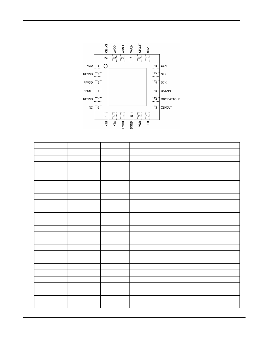
Pin Configuration
24-Pin MLF
Æ
(Top View)
Pin Number
Pin Name
Type
Pin Function
1 VDD
VDD
2 RFGND
RF
Ground
3 RFVDD
RF
VDD
4 RFOUT
O
RF
output
5 RFGND
RF
Ground
6 NC
Not
connected
7
XTB
O
Crystal oscillator output
8
XTA
I
Crystal oscillator input
9 DVDD
Digital
VDD
10 DGND
Digital
ground
11 VDD
VDD
12
LD
O
Lock Detect output
13
CLKOUT
O
Programmable Clock output
14
RDY/DATACLK
O
Transmit buffer Ready / Alternative Data clock
15
DATAIN
I
Alternative Data input
16 SCK I
SPI
clock
17 SIO
I/O
Serial
input/output
18
SEN
I
Serial programming interface enable
19
SRV
O
Service interrupt pin
20
CPOUT
O
Charge pump output
21
VARIN
I
VCO varactor input
22 AGND
Analog
ground
23 AVDD
Analog
VDD
24 CIBIAS O
Bias
25 HEATSINK
Ground

Micrel
MICRF405
April 2006
5
M9999-041906
(408) 955-1690
Absolute Maximum Ratings
(1)
Supply Voltage (V
DD
).........................................+3.7V
Voltage on any pin
(3)
(GND = 0V). .. -0.3V to 3.7V
Lead Temperature (soldering, 20sec.)............. 260∞C
Storage Temperature (T
s
) ................-55∞C to +150∞C
ESD Rating
(4)
All pins except pin 4...................................... 2 kV
Pin 4 (RFOUT)............................................ 200 V
Operating Ratings
(2)
Supply voltage (V
IN
)............................ +2.2V to +3.6V
RF Frequencies.......................... 290MHz to 980MHz
Data Rate (NRZ) ...........................................200kbps
Ambient Temperature (T
A
) ..............≠40∞C to +125∞C
Package Thermal Resistance
MLF
Æ
(
JA
) ............................................41.7∞C/W
Electrical Characteristics
f
RF
= 915MHz. V
DD
= 3.0V; T
A
= 25∞C, bold values indicate ≠40∞C< T
A
< +125∞C, unless noted.
Parameter Condition
Min
Typ
Max
Units
Freq_band=0
290
325
MHz
Freq_band=1
430
490
MHz
RF Frequency Operating Range
Freq_band=2-3
860
980
MHz
Power Supply
2.2
3.6
V
Power Down Current
0.3
µA
Standby Current
ClkOut_en=0
200
µA
PLL mode current
PA2-0=000, PA off
5.6
mA
VCO and PLL Section
Reference Frequency
4 40
MHz
1kHz loop filter bandwidth, Fphd=200kHz
7.0
ms
3kHz loop filter bandwidth, Fphd=500kHz
1.8
ms
PLL startup
30kHz loop filter bandwidth,
Fphd=1000kHz
140
µs
Standby-TX (PA on)
30kHz bandwidth
200
µs
Crystal Oscillator Start-Up Time
16MHz, 9pF load, XCO_Fast=1
300
µs
Charge Pump Current
V
CPOUT
= 1.2V, CP_CUR = 3
100
µA
Transmit Section
R
LOAD
= 250
, Pa2-0=111
10 dBm
Output Power
R
LOAD
= 250
, Pa2-0=001
-7 dBm
Over temperature range
1.5
dB
Output Power Tolerance
Over power supply range
3.0
dB
R
LOAD
= 150
, PA2-0=111
18 mA
R
LOAD
= 150
, PA2-0=001
9.6 mA
Tx Current Consumption
R
LOAD
= 150
, PA2-0=000
5.6 mA
ASK=7 (OOK)
60
dB
Modulation depth ASK/OOK
ASK=6
20
dB
Binary FSK Frequency Deviation
(5)
Bitrate
=
200kbps
300
kHz
VCO modulation
20 200
kbps
Divider modulation
20
kbps
Data Rate
(5)
ASK
50
kbps