MICRF610
868-870MHz ISM Band Transceiver
Module
RadioWireÆ is a trademark of Micrel, Inc.
Micrel Inc. ∑ 2180 Fortune Drive ∑ San Jose, CA 95131 ∑ USA ∑ tel +1 (
408
) 944-0800 ∑ fax + 1 (408) 474-1000 ∑ http://www.micrel.com
December 2005
M9999-120205
General Description
The MICRF610 is a self-contained frequency shift keying
(FSK) transceiver module, intended for use in half-duplex,
bidirectional RF links. The multi-channeled FSK
transceiver module is intended for UHF radio equipment in
compliance with European Telecommunication Standard
Institute (ETSI) specification EN300 220.
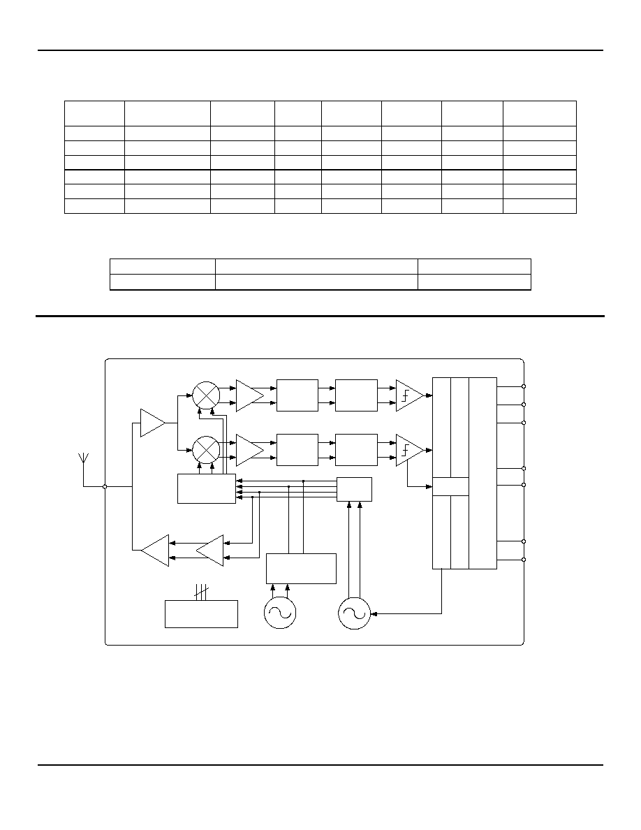
The transmitter consists of a fully programmable PLL
frequency synthesizer and power amplifier. The frequency
synthesizer consists of a voltage-controlled oscillator
(VCO), a crystal oscillator, dual modulus prescaler,
programmable frequency dividers, and a phase-detector.
The output power of the power amplifier can be
programmed to seven levels. A lock-detect circuit detects
when the PLL is in lock.
In receive mode, the PLL synthesizer generates the local
oscillator (LO) signal. The N, M, and A values that give the
LO frequency are stored in the N0, M0, and A0 registers.
The receiver is a zero intermediate frequency (IF) type that
makes channel filtering possible with low-power, integrated
low-pass filters. The receiver consists of a low noise
amplifier (LNA) that drives a quadrature mix pair. The
mixer outputs feed two identical signal channels in phase
quadrature. Each channel includes a pre-amplifier, a third
order Sallen-Key RC low-pass filter that protects the
following switched-capacitor filter from strong adjacent
channel signals, and a limiter. The main channel filter is a
switched-capacitor implementation of a six-pole elliptic low
pass filter. The cut-off frequency of the Sallen-Key RC filter
can be programmed to four different frequencies: 100kHz,
150kHz, 230kHz, and 350kHz. The I and Q channel
outputs are demodulated and produce a digital data
output. The demodulator detects the relative phase of the I
and the Q channel signal. If the I channel signal lags
behind the Q channel, the FSK tone frequency is above
the LO frequency (data "1"). If the I channel leads the Q
channel, then the FSK tone is below the LO frequency
(data "0"). The output of the receiver is available on the
DataIXO pin. A receive signal strength indicator (RSSI)
circuit indicates the received signal level. All support
documentation can be found on Micrel's web site at:
www.micrel.com.
RadioWire
Æ
Module
Features
∑ "Drop in" RF solution
∑ Small size: 11.5x14.1mm
∑ RF tested
∑ Low Power
∑ Surface Mountable
∑ Tape & Reel
∑ Digital Bit Synchronizer
∑ Received Signal Strength Indicator (RSSI)
∑ RX and TX power management
∑ Power down function
∑ Register read back function
Applications
∑ Telemetry
∑ Remote metering
∑ Wireless controller
∑ Remote data repeater
∑ Remote control systems
∑ Wireless modem
∑ Wireless security system

Micrel, Inc.
MICRF610
December 2005
2
M9999-120205
Contents
General Description ................................................................................................................................................................ 1
Features .................................................................................................................................................................................. 1
Applications ............................................................................................................................................................................. 1
Contents .................................................................................................................................................................................. 2
RadioWire
Æ
RF Module Selection Guide................................................................................................................................. 3
Ordering Information ............................................................................................................................................................... 3
Block Diagram......................................................................................................................................................................... 3
Pin Configuration..................................................................................................................................................................... 4
Pin Description ........................................................................................................................................................................ 4
Absolute Maximum Ratings
(1)
................................................................................................................................................. 5
Operating Ratings
(2)
................................................................................................................................................................ 5
Electrical Characteristics......................................................................................................................................................... 5
Programming........................................................................................................................................................................... 7
General ............................................................................................................................................................................... 7
Writing to the Control Registers in MICRF610 ................................................................................................................... 8
Writing to a Single Register ................................................................................................................................................ 8
Writing to All Registers ....................................................................................................................................................... 8
Writing to n Registers Having Incremental Addresses ....................................................................................................... 9
Reading from the Control Registers in MICRF610 ............................................................................................................. 9
Reading n Registers from MICRF610................................................................................................................................. 9
Programming Interface Timing.............................................................................................................................................. 10
Programming Summary.................................................................................................................................................... 11
Frequency Synthesizer ......................................................................................................................................................... 11
Crystal Oscillator (XCO) ................................................................................................................................................... 11
VCO .................................................................................................................................................................................. 12
Lock Detect ....................................................................................................................................................................... 12
Modes of Operation............................................................................................................................................................... 12
Transceiver Sync/Non-Synchronous Mode ...................................................................................................................... 13
Data Interface ................................................................................................................................................................... 13
Receiver ................................................................................................................................................................................ 13
Front End .......................................................................................................................................................................... 14
Sallen-Key Filters.............................................................................................................................................................. 14
Switched Capacitor Filter.................................................................................................................................................. 14
RSSI.................................................................................................................................................................................. 14
FEE ................................................................................................................................................................................... 15
Bit Synchronizer................................................................................................................................................................ 15
Transmitter ............................................................................................................................................................................ 16
Power Amplifier................................................................................................................................................................. 16
Frequency Modulation ...................................................................................................................................................... 16
Using the XCO-tune Bits ....................................................................................................................................................... 16
Application Circuit Illustration ................................................................................................................................................ 17
Assembling the MICRF610 ................................................................................................................................................... 17
Recommended Reflow Temperature Profile .................................................................................................................... 17
Shock/Vibration during Reflow.......................................................................................................................................... 17
Handassembling the MICRF610....................................................................................................................................... 17
Layout.................................................................................................................................................................................... 18
Recommended Land Pattern............................................................................................................................................ 18
Layout Considerations ...................................................................................................................................................... 18
Package Dimensions ............................................................................................................................................................ 19
Tape Dimensions .................................................................................................................................................................. 19
Micrel, Inc.
MICRF610
December 2005
5
M9999-120205
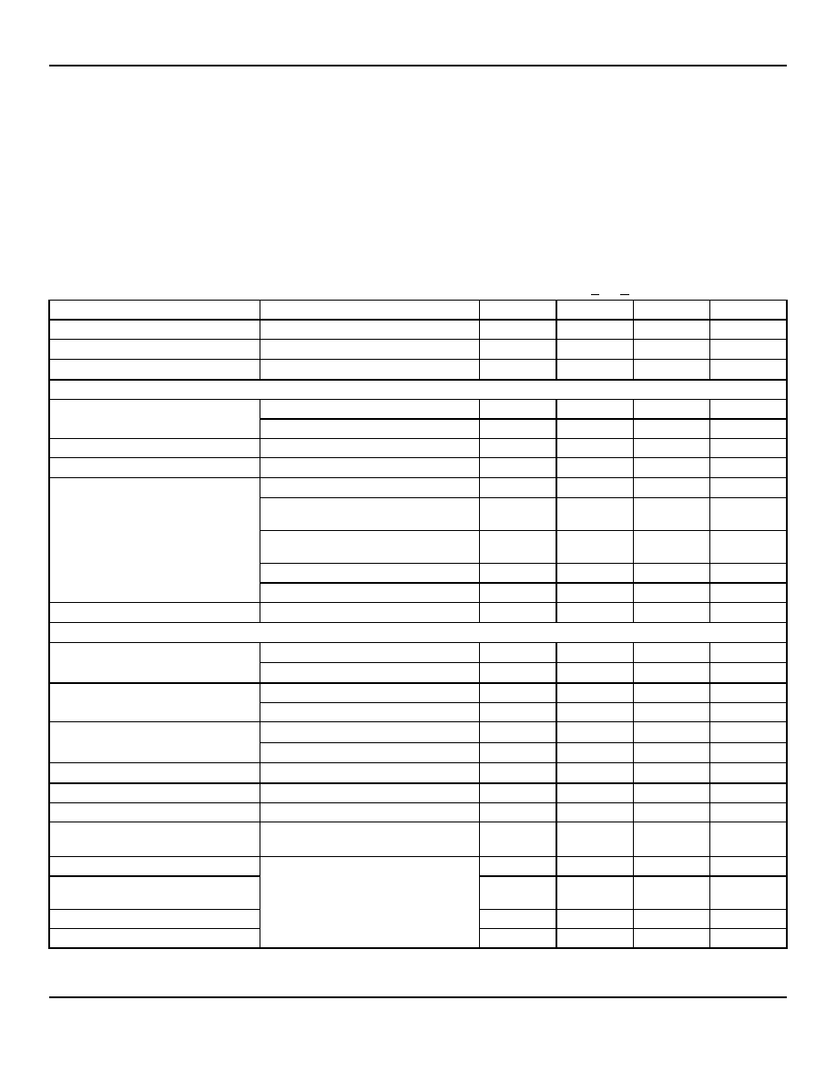
Absolute Maximum Ratings
(1)
Supply Voltage (V
DD
)...................................................+2.8V
Voltage on any pin (GND = 0V). ..................... -0.3V to 2.8V
Lead Temperature (soldering, 5 sec.)......................+225∞C
Storage Temperature (T
s
) ............................-30∞C to +85∞C
ESD Rating
(3)
..................................................................2kV
Operating Ratings
(2)
Supply voltage (V
IN
) ..................................+2.0V to +2.5V
RF Frequencies.................................868MHz to 870MHz
Data Rate (NRZ) ................................................ <15 kbps
Ambient Temperature (T
A
) .......................≠20∞C to +75∞C
Electrical Characteristics
f
RF
= 868.3MHz, Data rate = 15.2kbps, V
DD
= 2.5V; T
A
= 25∞C,
bold
values indicate ≠20∞C< T
A
< +75∞C, unless noted.
Parameter Condition
Min
Typ
Max
Units
Power Supply
2.0
2.5
V
Power Down Current
0.3
µA
Standby Current
280
µA
VCO and PLL Section
Tunable with on-chip cap bank
16
MHz
Crystal Oscillator Frequency
Tuning range
-30
+40
ppm
Crystal Initial Tolerance
-10 +10
ppm
Crystal Temperature Tolerance
-10 +10
ppm
Rx 868.3MHz ≠ Rx 868.95MHz
200
µs
Rx ≠ Tx, same frequency, measured @
frequency offset < 10kHz
150
µs
Tx ≠ Rx, same frequency, time to good
data
300
µs
Standby ≠ Rx,
2.0
ms
Switch Time
Standby ≠ Tx
2.0
ms
Crystal Oscillator Start-Up Time
XCO_tune=13
750
µs
Transmit Section
R
LOAD
= 50
, Pa2..0:111
8.5 dBm
Output Power
R
LOAD
= 50
, Pa2..0:001
-6
dBm
Over temperature range
1
dB
Output Power Tolerance
Over power supply range
3
dB
R
LOAD
= 50
, PA2_0: 111
26 mA
Tx Current Consumption
R
LOAD
= 50
, PA2_0: 001
14 mA
Tx Current Consumption Variation
R
LOAD
= 50
, PA2_0: 111
2.5 mA
Binary FSK Frequency Separation
(5)
Limited by receiver BW
20 400
kHz
Data Rate
NRZ
0
15.2
kbps
Occupied bandwidth
868.95MHz, 15.2kbps,
= 12
(
±85kHz), -36dBm (RBW=10kHz)
450 kHz
Harmonics 868
-30
dBm
Spurious Emission in Restricted
bands < 1GHz
-54
dBm
Spurious Emission < 1 GHz
-36
dBm
Spurious Emission > 1 GHz
ETSI EN 300-220
-30
dBm