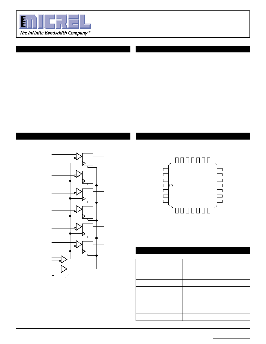
6-BIT REGISTER
DIFFERENTIAL DATA CLOCK
DESCRIPTION
The SY10/100E451 offer six D-type flip-flops with single-
ended outputs and differential data and clock inputs,
designed for use in new, high-performance ECL systems.
The registers are triggered by the rising edge of the CLK
input.
A logic HIGH on the Master Reset (MR) input resets all
outputs to a logic LOW. The V
BB
output is provided for use
as a reference voltage for single-ended reception of ECL
signals to that device only. When used for this purpose, it
is recommended that V
BB
is decoupled to V
CC
via a 0.01
µ
F
capacitor.
FEATURES
s
1100MHz min. toggle frequency
s
Extended 100E V
EE
range of ≠4.2V to ≠5.5V
s
Differential inputs: data and clock
s
V
BB
output for single-ended use
s
Asynchronous Master Reset
s
Fully compatible with industry standard 10KH,
100K ECL levels
s
Internal 75K
input pulldown resistors
s
Fully compatible with Motorola MC10E/100E451
s
Available in 28-pin PLCC package
SY10E451
SY100E451
FINAL
BLOCK DIAGRAM
D
R
D
R
D
R
D
R
D
R
D
R
Q
0
Q
1
Q
2
Q
3
Q
4
Q
5
MR
D
0
D
1
D
2
D
3
D
4
D
5
V
BB
CLK
/D
0
/CLK
/D
1
/D
2
/D
3
/D
4
/D
5
Pin
Function
D0≠D5
+ Data Input
/D0≠/D5
≠ Data Input
CLK
+ Clock Input
/CLK
≠ Clock Input
Q0≠Q5
Data Outputs
MR
Master Reset Input
V
BB
V
BB
Output
V
CCO
V
CC
to Output
PIN NAMES
PIN CONFIGURATION
TOP VIEW
PLCC
J28-1
26
27
28
1
2
3
4
18
17
16
15
14
13
12
25 24 23 22 21 20 19
5
6
7
8
9
10 11
VCC
Q5
Q4
Q1
Q3
Q2
VCCO
VCCO
D4
D5
D3
/D5
/D4
/D3
V
CCO
Q0
D1
D2
/D0
/D1
/D2
VEE
D0
MR
NC
CLK
VBB
/CLK
1
Rev.: D
Amendment: /0
Issue Date:
Feb. 19, 2001
2
SY10E451
SY100E451
Micrel
DC ELECTRICAL CHARACTERISTICS
T
A
= ≠40
∞
C
T
A
= 0
∞
C
T
A
= 25
∞
C
T
A
= +85
∞
C
Symbol
Parameter
Min.
Typ.
Max.
Min.
Typ.
Max.
Min.
Typ.
Max.
Min.
Typ.
Max.
Unit
V
BB
Output Reference
10E
≠1.38
--
≠1.27 ≠1.35
--
≠1.25 ≠1.31
--
≠1.19
V
Voltage
100E
≠1.38
--
≠1.26 ≠1.38
--
≠1.26 ≠1.38
--
≠1.26
I
IH
Input HIGH Current
--
--
150
--
--
150
--
--
150
µ
A
I
EE
Power Supply
10E
--
84
101
--
84
101
--
84
101
mA
Current
100E
--
84
101
--
84
101
--
97
116
V
CMR
Common Mode Range
(1)
≠2.0
--
≠0.4
≠2.0
--
≠0.4
≠2.0
--
≠0.4
V
PRODUCT ORDERING CODE
Ordering
Package
Operating
Code
Type
Range
SY10E451JI
J28-1
Industrial
SY10E451JITR
J28-1
Industrial
SY100E451JI
J28-1
Industrial
SY100E451JITR
J28-1
Industrial
V
EE
= V
EE
(Min.) to V
EE
(Max.); V
CC
= V
CCO
= GND
NOTE:
1. V
CMR
is referenced to the most psitive side of the differential input signal. Normal operation is obtained when the "HIGH" input is within the V
CMR
range
and the input swing is greater than V
PP
(min) and < 1V.
AC ELECTRICAL CHARACTERISTICS
T
A
= ≠40
∞
C
T
A
= 0
∞
C
T
A
= 25
∞
C
T
A
= +85
∞
C
Symbol
Parameter
Min.
Typ.
Max.
Min.
Typ.
Max.
Min.
Typ.
Max.
Min.
Typ.
Max.
Unit
f
MAX
Max. Toggle Frequency
1100
1400
--
1100
1400
--
1100
1400
--
MHz
t
PLH
Propagation Delay to
ps
t
PHL
Output
CLK (Diff)
475
650
800
475
650
800
475
650
800
CLK (SE)
425
650
850
425
650
850
425
650
850
MR
425
600
850
425
600
850
425
600
850
t
S
Set-up Time
D
150
≠100
--
150
≠100
--
150
≠100
--
ps
t
H
Hold Time
D
250
100
--
250
100
--
250
100
--
ps
V
PP (AC)
Minimum Input Swing
(1)
150
--
--
150
--
--
150
--
--
mV
t
RR
Reset Recovery Time
750
600
--
750
600
--
750
600
--
ps
t
PW
Minimum Pulse Width
400
--
--
400
--
--
400
--
--
ps
CLK, MR
t
skew
Within-Device Skew
(2)
--
100
--
--
100
--
--
100
--
ps
t
r
Rise/Fall Time
275
450
800
275
450
800
275
450
800
ps
t
f
20% to 80%
V
EE
= V
EE
(Min.) to V
EE
(Max.); V
CC
= V
CCO
= GND
NOTES:
1. Minimum input voltage for which AC parameters are guaranteed.
2. Within-device skew is defined as identical transitions on similar paths through a device.
Ordering
Package
Operating
Code
Type
Range
SY10E451JC
J28-1
Commercial
SY10E451JCTR
J28-1
Commercial
SY100E451JC
J28-1
Commercial
SY100E451JCTR
J28-1
Commercial
3
SY10E451
SY100E451
Micrel
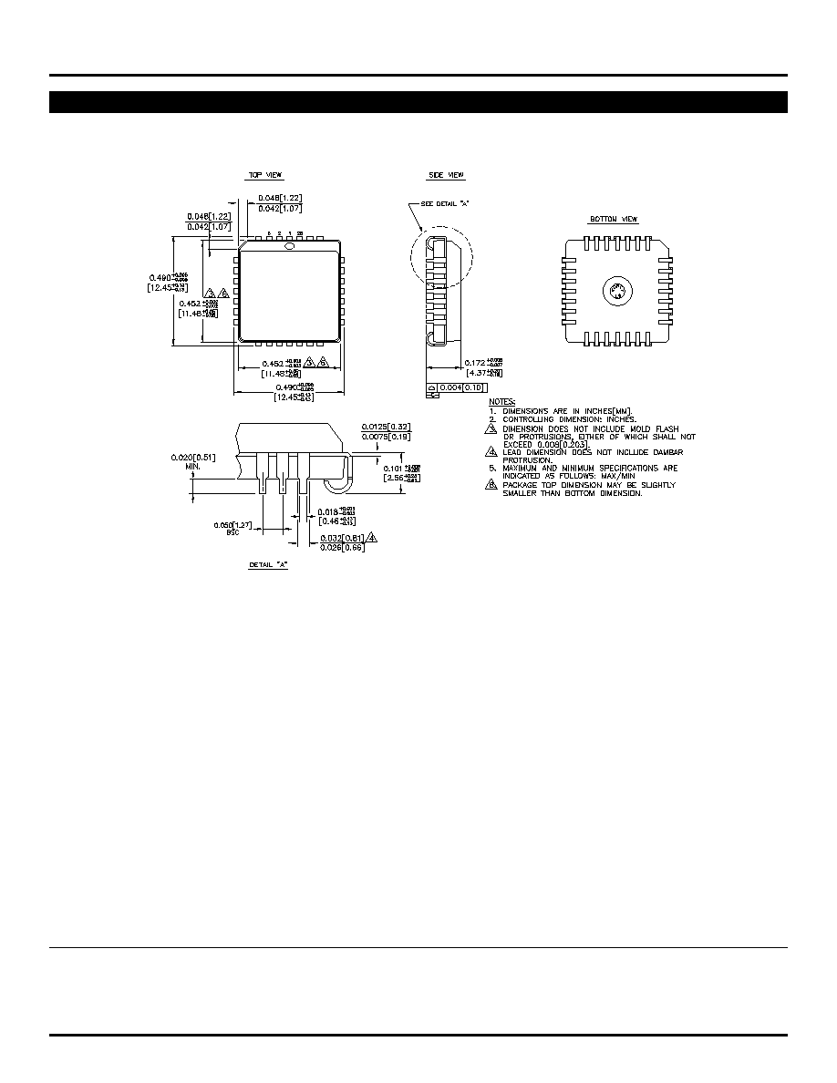
28 LEAD PLCC (J28-1)
Rev. 03
MICREL-SYNERGY
3250 SCOTT BOULEVARD
SANTA CLARA
CA 95054
USA
TEL
+ 1 (408) 980-9191
FAX
+ 1 (408) 914-7878
WEB
http://www.micrel.com
This information is believed to be accurate and reliable, however no responsibility is assumed by Micrel for its use nor for any infringement of patents or
other rights of third parties resulting from its use. No license is granted by implication or otherwise under any patent or patent right of Micrel Inc.
© 2001 Micrel Incorporated