DESCRIPTION
s
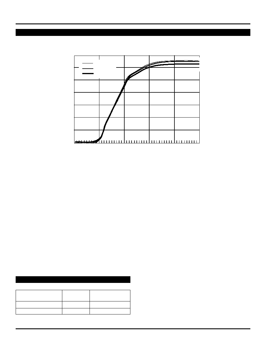
Up to 1.25Gbps operation
s
75mA peak drive current
s
Separate modulation control
s
Separate output enable for laser safety
s
Differential inputs for data
s
75K
input pulldown resistor
s
Single power supply
s
Available in 16-pin SOIC package
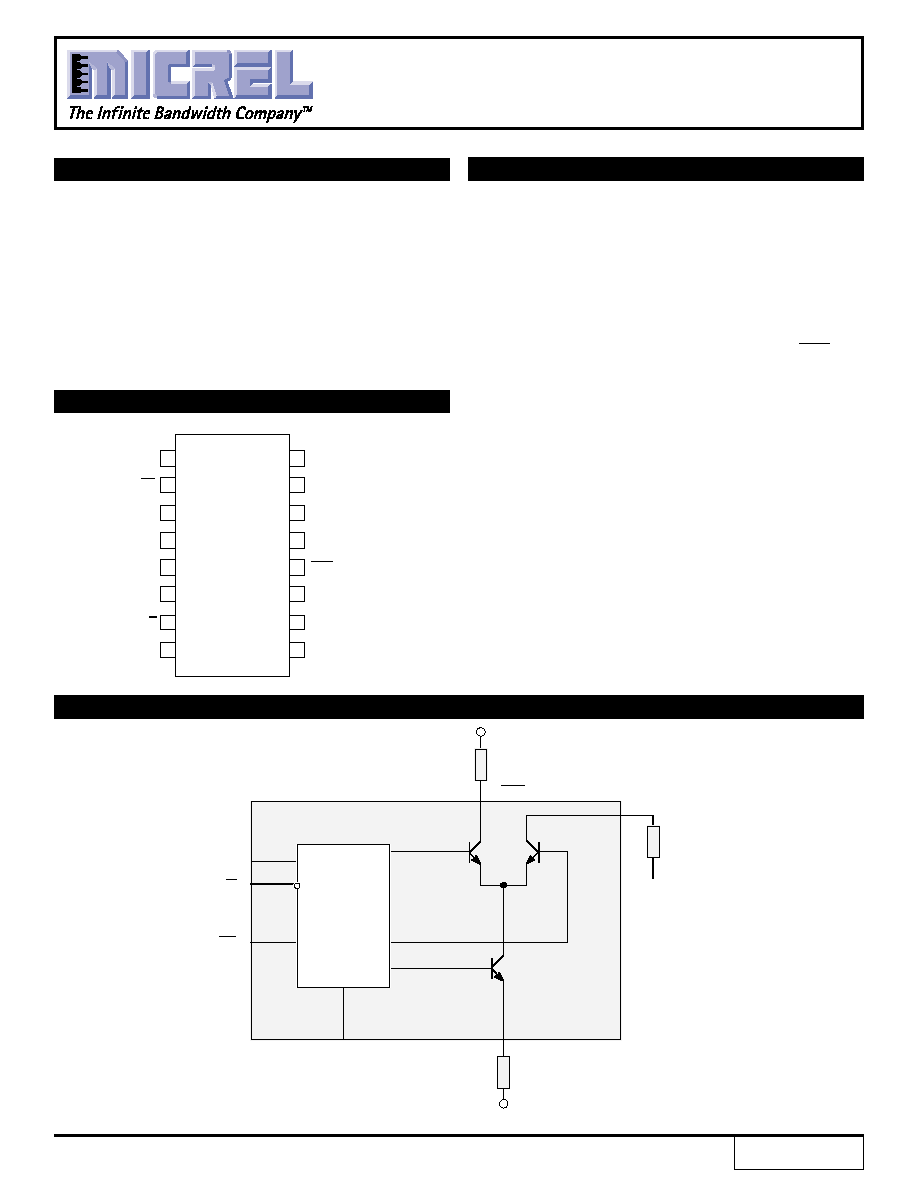
The SY100EL1003 is a high speed current source for
driving a semiconductor laser diode in optical transmission
applications. The output current modulation is DC ≠
voltage controlled. The modulation current is disabled
when output enable is HIGH.
The device incorporates complementary open collector
outputs with a capability of driving peak current of 75mA.
The laser driver current is adjustable by selection of R
SET
.
The resistor R
EXT
must be placed between OUT and
V
CC
to dissipate the worst case power. R
SER
is
recommended to fix laser diode matching issues.
The SY100EL1003 utilizes the high performance
bipolar ASSET technology.
FEATURES
LASER DIODE DRIVER
WITH OUTPUT ENABLE
PIN CONFIGURATION
PRELIMINARY
SY100EL1003
BLOCK DIAGRAM
Rev.: D
Amendment: /0
Issue Date: August, 1998
D
EN
V
CC
R
EXT
OUT
OUT
V
BB
R
SET
V
EE
R
SER
to Laser Diode
MC
Modulation Control
D
Internal Logic
BIAS
Control
R
SET
NC
16
15
14
13
12
11
10
9
1
2
3
4
5
6
7
8
EN
N/C
R
SET
V
CCO
D
D
NC
V
CC
NC
MC
OUT
OUT
V
BB
NC
V
EE
Top View
SOIC
Z16-2
1
2
PRELIMINARY
SY100EL1003
Micrel
D
D
EN
OUT
OUT
L
H
L
H
L
H
L
L
L
H
X
X
H
H
L
NOTE:
1. L = LOW, H = HIGH, X = don't care
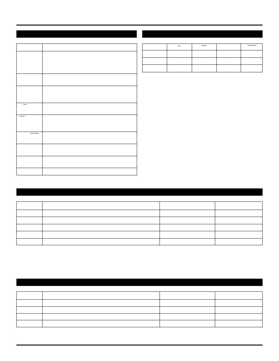
Pin
Function
V
CC
, V
CCO
Separate positive power supply pins help
to isolate sensitive circuitry from noise
generating function. +5V for PECL operation
or ground for ECL operation.
V
EE
Most negative power supply input. Ground
for PECL operation or -5V for ECL operation.
V
BB
This pin provides a reference voltage for use
in single ended applications or when the
input signal is AC coupled into the device.
D,D
These differential ECL/PECL 100K
compatible inputs receive NRZ data.
EN
This ECL/PECL 100K compatible input enables
Laser Driver - modulation current transitions to
zero when asserted HIGH.
OUT, OUT
Open collector outputs from the modulation
buffer drive these differential current outputs.
MC
An external voltage sets the main value of
modulation current I
O
.
R
SET
An external resistor sets the source current
for modulation I
mod
.
NC
These pins are not connected.
Symbol
Rating
Value
Unit
V
EE
Power Supply Voltage (V
CC
= 0V)
0 to -7.0
V
V
I
Input Voltage (V
CC
= 0V)
0 to -6.0
V
I
O
Output Current
75
mA
T
A
Operating Temperature Range
≠40 to +85
∞
∞
C
P
tot
Power Dissipation
500
mW
ABSOLUTE MAXIMUM RATINGS
(1)
NOTE:
1. Permanent device damage may occur if ABSOLUTE MAXIMUM RATINGS are exceeded. This is a stress rating only and functional operation is not implied
at conditions other than those detailed in the operational sections of this data sheet. Exposure to ABSOLUTE MAXIMUM RATlNG conditions for extended
periods may affect device reliability.
PIN NAMES
TRUTH TABLE
(1)
Symbol
Rating
Value
Unit
V
EE
Power Supply Voltage
≠4.75 to -5.25
V
R
SET
Resistor to Adjust Current
10 to 100
R
EXT
Resistor to Dissipate Power
10 to 50
R
SER
Laser Diode Serial Resistor
0 to 50
OPERATIONING CONDITIONS
(1)
NOTE:
1. The voltage drop across R
EXT
and R
SER
should not be greater than 2V.
5
PRELIMINARY
SY100EL1003
Micrel
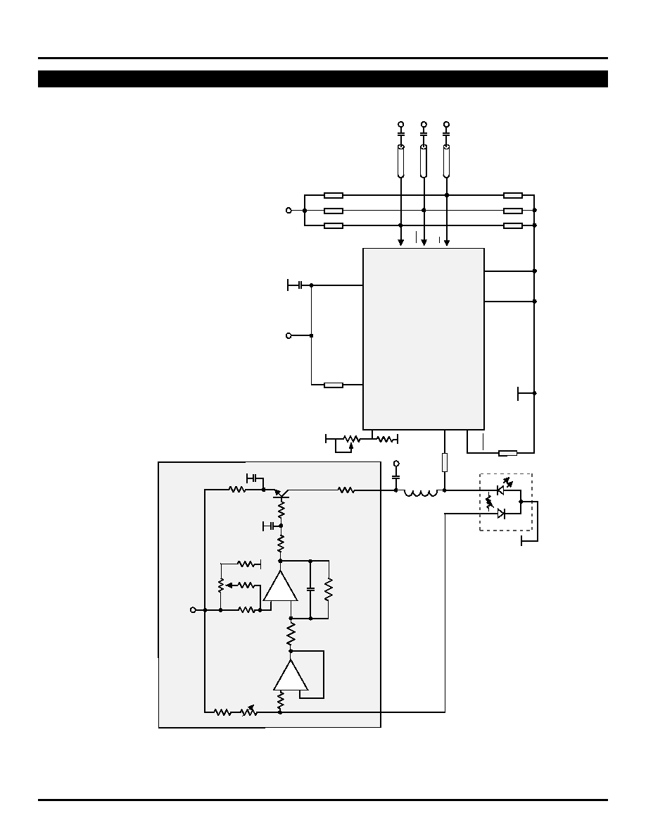
APPLICATION EXAMPLE
NOTES:
1.
Split 100K ECL terminations are 82
and 130
to V
CC
and V
EE
respectively.
2.
Recommended power supply bypass capacitors are 0.1
µ
F with optional 10
µ
F Tantalum in parallel.
3.
It is required to use high frequency design techniques for board layout. A double sided or multilayer board is recommended i
n conjunction with a low
impedance ground plane and properly terminated transmission lines for all signal paths.
4.
V
BB
voltage pin may be used as reference for single ended input applications.
V
CC
R
SET
V
EE
V
CCO
D
50
COAX
50
COAX
R
EXT
R
SET
SY100EL1003
V
EE
V
EE
OUT
R
SER
V
EE
LASER MODULE
INPUTS
50
COAX
LASER BIAS / APC CONTROL
470k
0.1µF
0.1µF
1k
1k
0.1µF
10k
1k
B
750
47k
47k
4.7k
47k
10k
A
D
EN
OUT
0.02µF
V
EE
V
CC
V
CC
V
CC
IC
1
= IC
2
= LM324
V
EE
=
≠
5.0V
V
CC
= 0V
IC
2
≠
+
IC
1
≠
+
0.1µH
V
CC
V
CC
V
CC
0.1µF
130
82
MC
V
CC
V
EE
10k
10
24