Pin
Function
D
Data Inputs
Q
Data Outputs
V
BB
Reference Voltage Output
V
CTRL
Output Swing Control
DESCRIPTION
FEATURES
5V/3.3V VARIABLE
OUTPUT SWING
DIFFERENTIAL RECEIVER
SY100EL16VS
s
3.3V and 5V power supply options
s
High bandwidth output transitions
s
Internal 75K
pull-down resistors on inputs
s
Functionally equivalent to SY100EL16V with variable
output swing
s
Improved output waveform characteristics
s
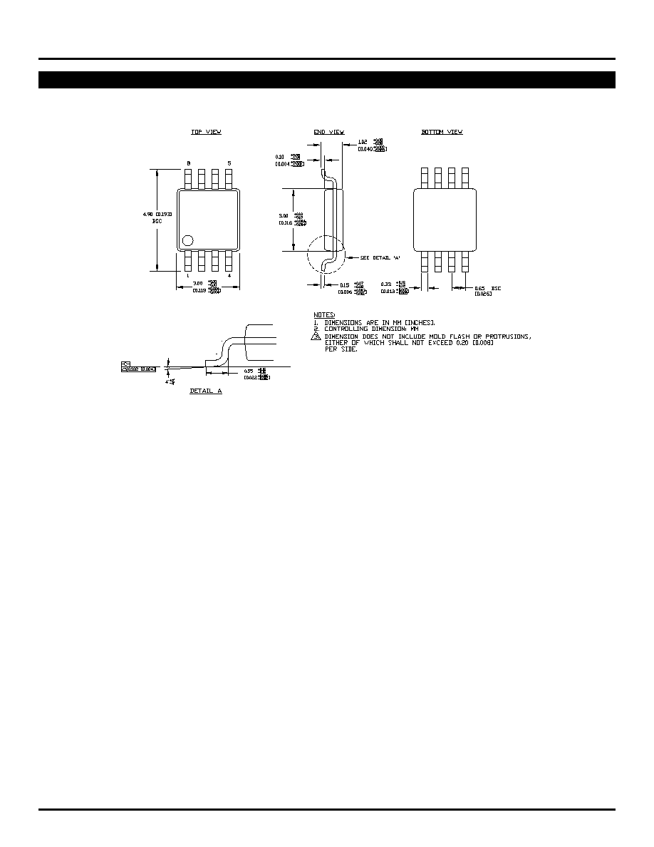
Available in 8-pin SOIC and 8-pin (3mm) MSOP
The SY100EL16VS are differential receivers with
variable output swing. The devices are functionally
equivalent to the EL16V devices with an input that control
the amplitude of the outputs.
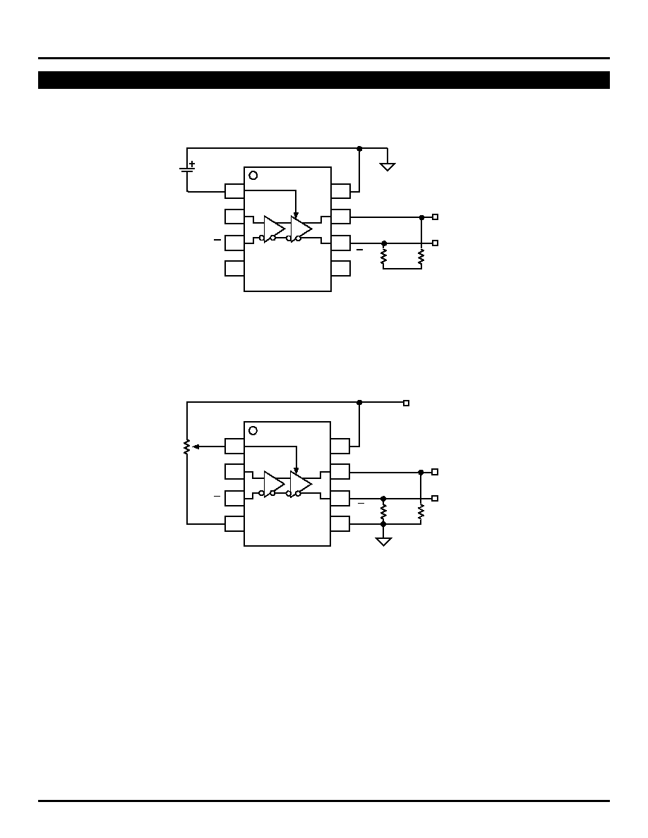
The operational range of the EL16VS control input is
from V
BB
(max. swing) to V
CC
(min. swing). Simple control
of the output swing can be obtained by a variable resistor
between the V
BB
pin and V
CC
with the wiper driving
V
CTRL
.
The EL16VS provides a V
BB
output for either single-
ended use or as a DC bias for AC coupling to the device.
The V
BB
pin should be used only as a bias for the EL16VS
as its current sink/source capability is limited. Whenever
used, the V
BB
pin should be bypassed to ground via a
0.01
µ
F capacitor.
Under open input conditions (pulled to V
EE
), internal
input clamps will force the Q output LOW.
PIN NAMES
PIN CONFIGURATION/BLOCK DIAGRAM
Figure 1. Typical Voltage Output Swing
V
CC
= 3.3V or 5V
TYPICAL VOLTAGE OUTPUT SWING
0
10
20
30
40
50
60
70
80
90
100
0 0.2 0.4 0.6 0.8 1.0 1.2 1.4 1.6
VOLTAGE SWING (%)
V
CC
≠ V
CTRL
-40
∞
C
+45
∞
C
+105
∞
C
1
2
3
4
8
V
CC
Q
V
EE
D
V
BB
Q
V
CTRL
D
7
6
5
1
Rev.: B
Amendment: /1
Issue Date:
July 2000
2
SY100EL16VS
Micrel
NOTES:
1. Parametric values specified at:
100EL16VS Series:
≠3.0V to ≠5.5V.
2. If V
CTRL
is an open circuit, use the V
OH
(max. & min.) and V
OL
(V
CTRL
= V
BB
: max only) limits.
3. V
CC
V
CTRL
V
EE
.
DC ELECTRICAL CHARACTERISTICS
(1)
T
A =
≠40
∞
C
T
A =
0
∞
C
T
A =
+25
∞
C
T
A =
+85
∞
C
Symbol
Parameter
Min.
Typ.
Max.
Min.
Typ.
Max.
Min.
Typ.
Max.
Min.
Typ.
Max. Unit
I
EE
Power Supply Current
--
18
22
9
18
22
9
18
22
9
21
26
mA
V
BB
Output Reference
-1.38
--
-1.26
-1.38
--
-1.26
-1.38
--
-1.26
-1.38
--
-1.26
V
Voltage
I
IH
Input HIGH
-D, D
--
--
150
--
--
150
--
--
150
--
--
150
µ
A
Current
-V
CTRL
--
--
40
--
--
40
--
--
40
--
--
40
V
OL
Output LOW Voltage
(2)
-1890
--
-1620 -1870
--
-1680 -1870 -1775 -1680 -1870
--
-1680
mV
V
CTRL
= V
BB
V
OL
Output LOW Voltage
(2)
-1180
--
-975
-1135
--
-990
-1135 -1065
-990
-1135
--
-990
mV
V
CTRL
= V
CC
V
OH
Output HIGH Voltage
(3)
-1085
--
-880
-1025
--
-880
-1025
-955
-880
-1025
--
-880
mV
V
EE
= V
EE
(Min.) to V
EE
(Max.); V
CC
= GND
NOTES:
1. Parametric values specified at:
100EL16VS Series:
≠3.0V to ≠5.5V.
2. Duty cycle skew is the difference between a t
PLH
and t
PHL
propagation delay through a device.
3. Minimum input swing for which AC parameters are guaranteed. The device has a DC gain of
40 when output has a full swing.
4. The CMR range is referenced to the most positive side of the differential input signal. Normal operation is obtained if the HIGH level falls within the specified
range and the peak-to-peak voltage lies between V
PP
min. and 1V. The lower end of the CMR range varies 1:1 with V
EE
. The numbers in the spec table
assume a nominal V
EE
= ≠3.3V. Note for PECL operation, the V
CMR
(min) will be fixed at 3.3V ≠ |V
CMR
(min)|.
V
EE
= V
EE
(Min.) to V
EE
(Max.); V
CC
= GND
T
A =
≠40
∞
C
T
A =
0
∞
C
T
A =
+25
∞
C
T
A =
+85
∞
C
Symbol
Parameter
Min.
Typ.
Max.
Min.
Typ.
Max.
Min.
Typ.
Max.
Min.
Typ.
Max. Unit
t
PLH
Propagation
D (Diff)
175
--
325
175
--
325
175
--
325
205
--
355
ps
t
PHL
Delay to Output
D (SE)
125
250
425
125
250
375
125
250
375
155
280
405
t
skew
Duty Cycle Skew
(2)
(Diff)
--
5
--
--
5
20
--
5
20
--
5
20
ps
V
PP
Minimum Input Swing
(3)
150
--
--
150
--
--
150
--
--
150
--
--
mV
V
CMR
Common Mode Range
(4)
-1.3
--
-0.4
-1.4
--
-0.4
-1.4
--
-0.4
-1.4
--
-0.4
V
t
r
Output Rise/Fall Times Q
--
160
260
--
160
260
--
160
260
--
160
260
ps
t
f
(20% to 80%)
AC ELECTRICAL CHARACTERISTICS
(1)
PRODUCT ORDERING CODE
Ordering
Package
Operating
V
EE
Range
Code
Type
Range
(V)
SY100EL16VSKC
K8-1
Commercial
-3.0 to -5.5
SY100EL16VSZC
Z8-1
Commercial
-3.0 to -5.5
5
SY100EL16VS
Micrel
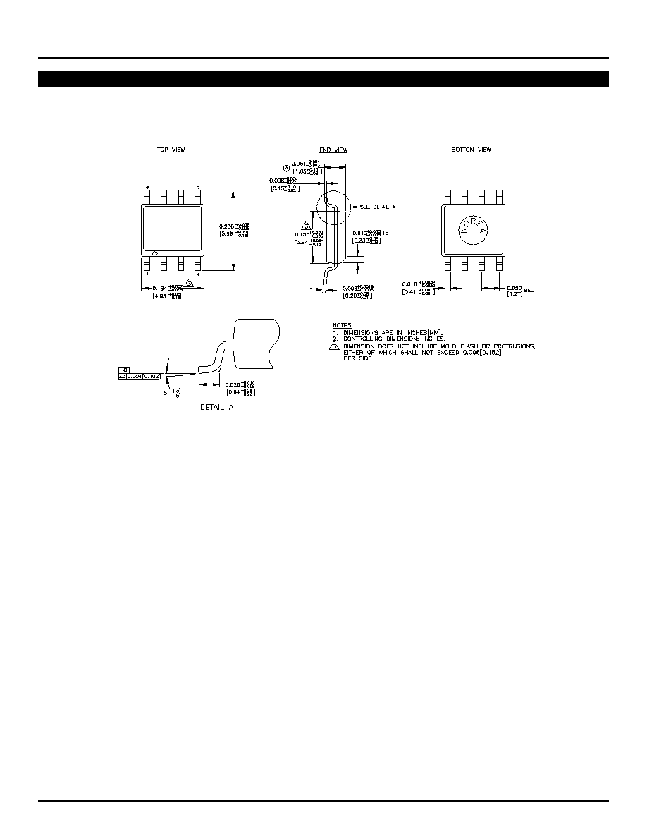
8 LEAD SOIC .150" WIDE (Z8-1)
Rev. 03
MICREL-SYNERGY
3250 SCOTT BOULEVARD
SANTA CLARA
CA 95054
USA
TEL
+ 1 (408) 980-9191
FAX
+ 1 (408) 914-7878
WEB
http://www.micrel.com
This information is believed to be accurate and reliable, however no responsibility is assumed by Micrel for its use nor for any infringement of patents or
other rights of third parties resulting from its use. No license is granted by implication or otherwise under any patent or patent right of Micrel Inc.
© 2000 Micrel Incorporated