DESCRIPTION
s
3.3V and 5V power supply options
s
510ps propagation delay
s
3.0GHz toggle frequency
s
High bandwidth output transistions
s
Internal 75K
input pull-down resistors
s
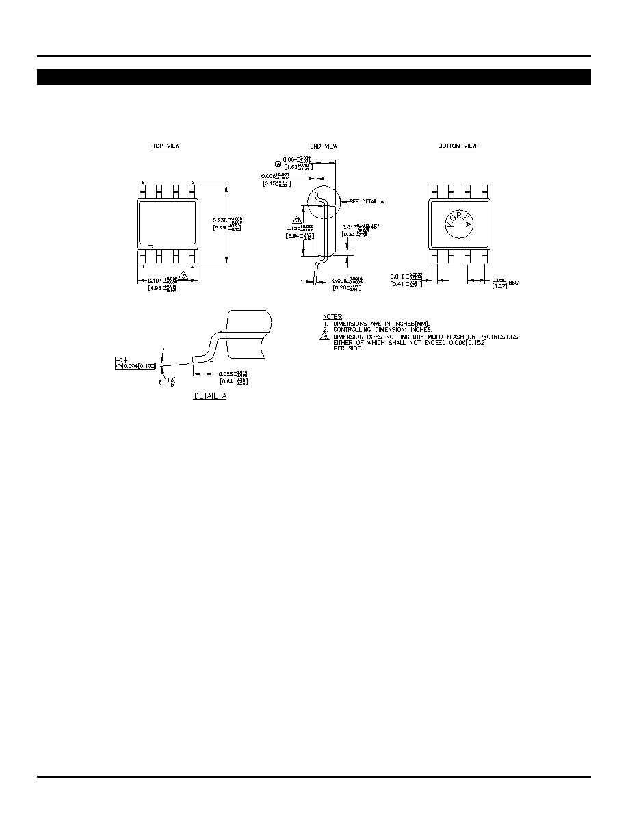
Available in 8-pin SOIC package
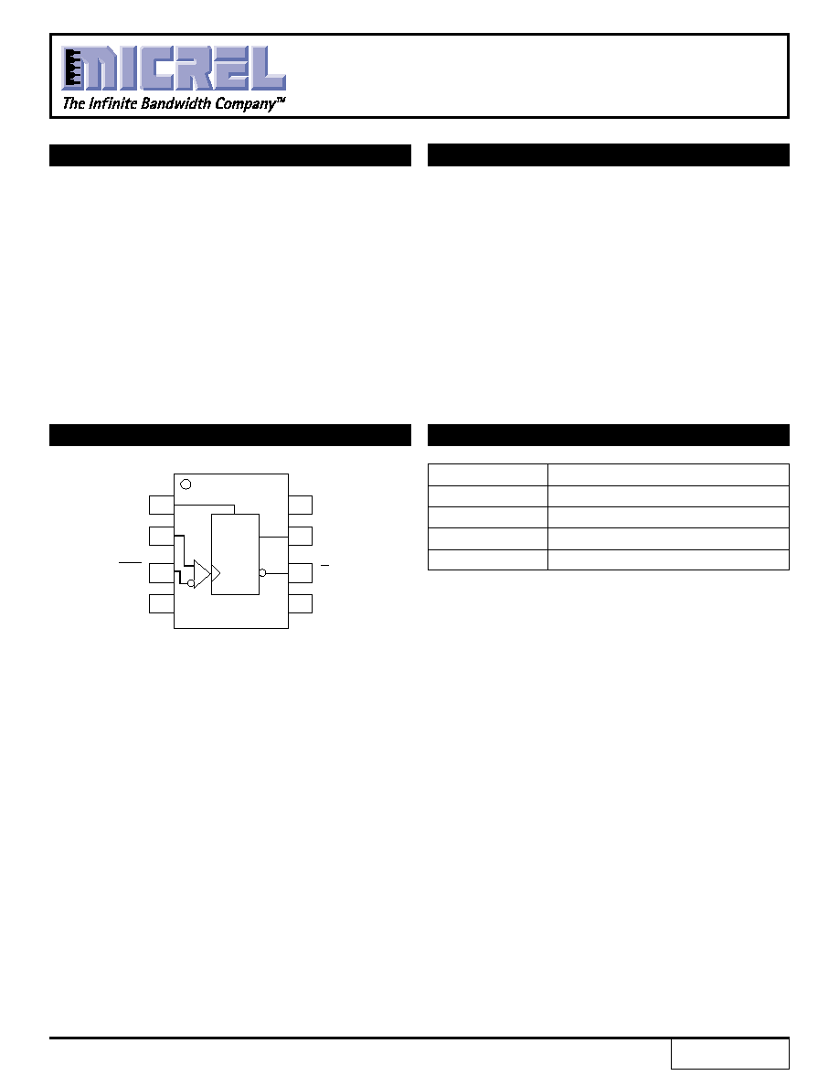
The SY10/100EL32V are integrated
˜
2 dividers. The
differential clock inputs and the V
BB
allow a differential,
single-ended or AC-coupled interface to the device. If
used, the V
BB
output should be bypassed to ground with
a 0.01
µ
F capacitor. Also note that the V
BB
is designed to
be used as an input bias on the EL32V only; the V
BB
output has limited current sink and source capability.
The reset pin is asynchronous and is asserted on the
rising edge. Upon power-on, the internal flip-flop will attain
a random state; the reset allows for the synchronization
of multiple EL32Vs in a system.
FEATURES
PIN CONFIGURATION/BLOCK DIAGRAM
PIN NAMES
5V/3.3V
˜
2 DIVIDER
SOIC
TOP VIEW
Pin
Function
CLK
Clock Inputs
Reset
Asynchronous Reset
V
BB
Reference Voltage Output
Q
Data Outputs
1
2
3
4
5
6
7
8
Reset
V
CC
Q
V
EE
CLK
V
BB
Q
R
CLK
˜
2
Rev.: C
Amendment: /0
Issue Date: August, 1998
ClockWorksTM
SY10EL32V
SY100EL32V
1
2
ClockWorksTM
SY10EL32V
SY100EL32V
Micrel
T
A =
≠40
∞
C
T
A =
0
∞
C
T
A =
+25
∞
C
T
A =
+85
∞
C
Symbol
Parameter
Min.
Typ.
Max.
Min.
Typ.
Max.
Min.
Typ.
Max.
Min.
Typ.
Max.
Unit
f
MAX
Maximum Toggle
2.2
3.0
--
2.6
3.0
--
2.6
3.0
--
2.6
3.0
--
GHz
Frequency
t
PLH
Prop Delay to Output D
360
500
640
410
500
590
420
510
600
450
540
630
ps
t
PHL
Reset to Q
390
540
690
440
540
640
440
540
640
450
550
650
V
PP
Minimum Input Swing
(2)
150
--
--
150
--
--
150
--
--
150
--
--
mV
V
CMR
Common Mode Range
(3)
≠1.3
--
≠0.4
≠1.4
--
≠0.4
≠1.4
--
≠0.4
≠1.4
--
≠0.4
V
t
r
Output Rise/Fall Times Q
100
225
350
100
225
350
100
225
350
100
225
350
ps
t
f
(20% to 80%)
AC ELECTRICAL CHARACTERISTICS
(1)
NOTES:
1. Parametric values specified at:
10/100EL32V Series:
-3.0V to -5.5V.
2. Minimum input swing for which AC parameters are guaranteed. The device has a DC gain of
40.
3. The CMR range is referenced to the most positive side of the differential input signal. Normal operation is obtained if the HIGH level falls within the specified
range and the peak-to-peak voltage lies between V
PP
min. and 1V. The lower end of the CMR range varies 1:1 with V
EE
. The numbers in the spec table
assume a nominal V
EE
= ≠3.3V. Note for PECL operation, the V
CMR
(min) will be fixed at 3.3V ≠ |V
CMR
(min)|.
DC ELECTRICAL CHARACTERISTICS
(1)
T
A =
≠40
∞
C
T
A =
0
∞
C
T
A =
+25
∞
C
T
A =
+85
∞
C
Symbol
Parameter
Min.
Typ.
Max.
Min.
Typ.
Max.
Min.
Typ.
Max.
Min.
Typ.
Max.
Unit
I
EE
Power Supply
mA
Current
10EL
--
25
30
--
25
30
--
25
30
--
25
30
100EL
--
25
30
--
25
30
--
25
30
--
29
35
V
BB
Output Reference
V
Voltage
10EL ≠1.43
--
≠1.30
≠1.38
--
≠1.27 ≠1.35
--
≠1.25
≠1.31
--
≠1.19
100EL ≠1.38
--
≠1.26
≠1.38
--
≠1.26 ≠1.38
--
≠1.26
≠1.38
--
≠1.26
I
IH
Input HIGH Current
--
--
150
--
--
150
--
--
150
--
--
150
µ
A
V
EE
= V
EE
(Min.) to V
EE
(Max.); V
CC
= GND
V
EE
= V
EE
(Min.) to V
EE
(Max.); V
CC
= GND
NOTE:
1. Parametric values specified at:
10/100EL32V Series:
-3.0V to -5.5V.
PRODUCT ORDERING CODE
Ordering
Package
Operating
VEE Range
Code
Type
Range
(V)
SY10EL32VZC
Z8-1
Commercial
-3.0 to -5.5
SY10EL32VZCTR
Z8-1
Commercial
-3.0 to -5.5
SY100EL32VZC
Z8-1
Commercial
-3.0 to -5.5
SY100EL32VZCTR
Z8-1
Commercial
-3.0 to -5.5

4
ClockWorksTM
SY10EL32V
SY100EL32V
Micrel
MICREL-SYNERGY
3250 SCOTT BOULEVARD
SANTA CLARA
CA 95054
USA
TEL
+ 1 (408) 980-9191
FAX
+ 1 (408) 914-7878
WEB
http://www.micrel.com
This information is believed to be accurate and reliable, however no responsibility is assumed by Micrel for its use nor for any infringement of patents or
other rights of third parties resulting from its use. No license is granted by implication or otherwise under any patent or patent right of Micrel Inc.
© 2000 Micrel Incorporated