DESCRIPTION
s
365ps propagation delay
s
2.0GHz toggle frequency
s
Internal 75K
input pull-down resistors
s
Available in 8-pin SOIC package
The SY10/100EL52 are differential data, differential
clock D flip-flops. These devices are functionally
equivalent to the E452 devices, with higher performance
capabilities. With propagation delays and output transition
times significantly faster than the E452, the EL52 is ideally
suited for those applications which require the ultimate
in AC performance.
Data enters the master portion of the flip-flop when
the clock is LOW and is transferred to the slave, and
thus the outputs, upon a positive transition of the clock.
The differential clock inputs also allow the EL52 to be
used as a negative edge triggered device.
The EL52 employs input clamping circuitry so that,
under open input conditions (pulled down to V
EE
), the
outputs of the device will remain stable.
FEATURES
DIFFERENTIAL DATA AND
CLOCK D FLIP-FLOP
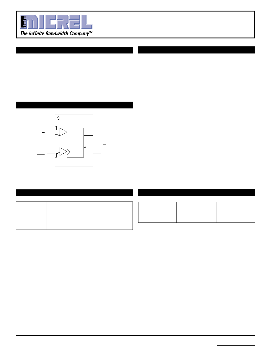
PIN CONFIGURATION/BLOCK DIAGRAM
D
CLK
Q
L
Z
L
H
Z
H
NOTE:
1. Z = LOW-to-HIGH transition.
SOIC
TOP VIEW
Pin
Function
D
Data Input
CLK
Clock Input
Q
Data Output
1
2
3
4
5
6
7
8
D
V
CC
Q
V
EE
Q
CLK
Flip-Flop
D
CLK
D
Rev.: F
Amendment: /0
Issue Date:
August, 1998
SY10EL52
SY100EL52
TRUTH TABLE
(1)
PIN NAMES
1

2
SY10EL52
SY100EL52
Micrel
AC ELECTRICAL CHARACTERISTICS
V
EE
= V
EE
(Min.) to V
EE
(Max.); V
CC
= GND
T
A =
≠40
∞
C
T
A =
0
∞
C
T
A =
+25
∞
C
T
A =
+85
∞
C
Symbol
Parameter
Min.
Typ.
Max.
Min.
Typ.
Max.
Min.
Typ.
Max.
Min.
Typ.
Max.
Unit
f
MAX
Maximum Toggle
1.8
2.5
--
2.2
2.8
--
2.2
2.8
--
2.2
2.8
--
GHz
Frequency
t
PLH
Propagation Delay to
ps
t
PHL
Output
CLK
235
335
515
275
365
465
275
365
465
320
410
510
t
S
Set-up Time
125
0
--
125
0
--
125
0
--
125
0
--
ps
t
H
Hold Time
150
50
--
150
50
--
150
50
--
150
50
--
ps
t
PW
Minimum Pulse Width
400
--
--
400
--
--
400
--
--
400
--
--
ps
V
PP
Minimum Input Swing
(1)
150
--
--
150
--
--
150
--
--
150
--
--
mV
V
CMR
Common Mode Range
(2)
V
D (10EL)
≠0.4
--
≠1.6
≠0.4
--
≠1.6
≠0.4
--
≠1.6
≠0.4
--
≠1.6
D (100EL)
≠0.4
--
≠1.2
≠0.4
--
≠1.2
≠0.4
--
≠1.2
≠0.4
--
≠1.2
CLK (10EL)
≠0.6
--
(3)
≠0.6
--
(3)
≠0.6
--
(3)
≠0.6
--
(3)
CLK (100EL)
≠0.8
--
(3)
≠0.8
--
(3)
≠0.8
--
(3)
≠0.8
--
(3)
t
r
Output Rise/Fall Times Q
100
225
350
100
225
350
100
225
350
100
225
350
ps
t
f
(20% to 80%)
PRODUCT ORDERING CODE
Ordering
Package
Operating
Code
Type
Range
SY10EL52ZC
Z8-1
Commercial
SY10EL52ZCTR
Z8-1
Commercial
SY100EL52ZC
Z8-1
Commercial
SY100EL52ZCTR
Z8-1
Commercial
NOTES:
1. Minimum input swing for which AC parameters are guaranteed.
2. The CMR range is referenced to the most positive side of the differential input signal. Normal operation is obtained if the HIGH level falls within the specified
range and the peak-to-peak voltage lies between V
PP
min. and 1V.
3. The lower end of the CMR range is dependent on V
EE
and is equal to V
EE
+ 3.0V.
DC ELECTRICAL CHARACTERISTICS
T
A =
≠40
∞
C
T
A =
0
∞
C
T
A =
+25
∞
C
T
A =
+85
∞
C
Symbol
Parameter
Min.
Typ.
Max.
Min.
Typ.
Max.
Min.
Typ.
Max.
Min.
Typ.
Max.
Unit
I
EE
Power Supply
10EL
--
21
25
17
21
25
17
21
25
17
21
25
mA
Current
100EL
--
21
25
17
21
25
17
21
25
19
24
29
V
EE
Power Supply
10EL
≠4.75
≠5.2
≠5.5
≠4.75
≠5.2
≠5.5
≠4.75
≠5.2
≠5.5
≠4.75
≠5.2
≠5.5
V
Voltage
100EL
≠4.20
≠4.5
≠5.5
≠4.20
≠4.5
≠5.5
≠4.20
≠4.5
≠5.5
≠4.20
≠4.5
≠5.5
I
IH
Input HIGH Current
--
--
150
--
--
150
--
--
150
--
--
150
µ
A
V
EE
= V
EE
(Min.) to V
EE
(Max.); V
CC
= GND

4
SY10EL52
SY100EL52
Micrel
MICREL-SYNERGY
3250 SCOTT BOULEVARD
SANTA CLARA
CA 95054
USA
TEL
+ 1 (408) 980-9191
FAX
+ 1 (408) 914-7878
WEB
http://www.micrel.com
This information is believed to be accurate and reliable, however no responsibility is assumed by Micrel for its use nor for any infringement of patents or
other rights of third parties resulting from its use. No license is granted by implication or otherwise under any patent or patent right of Micrel Inc.
© 2000 Micrel Incorporated


