
DESCRIPTION
s
2.6ns typical propagation delay
s
Differential ECL inputs
s
24mA TTL outputs
s
Flow-through pinouts
s
Available in 8-pin SOIC package
The SY100ELT25 is a differential ECL-to-TTL
translator. Because ECL levels are used, a +5V, ≠5.2V
(or ≠4.5V) and ground are required. The small outline 8-
lead SOIC package and the single gate of the ELT25
makes it ideal for those applications where performance,
space and low power are at a premium.
The V
BB
output allows the ELT25 to also be used in a
single-ended input mode. In this mode the V
BB
output is
tied to the D input for a non-inverting buffer or the D
input for an inverting buffer. If used the V
BB
pin should
be bypassed to ground via a 0.01
µ
F capacitor.
FEATURES
DIFFERENTIAL
ECL-to-TTL
TRANSLATOR
PIN NAMES
PIN CONFIGURATION/BLOCK DIAGRAM
Pin
Function
Q
TTL Output
D
Differential ECL Inputs
V
CC
Positive Supply
V
EE
Negative Supply
V
BB
Reference Output
GND
Ground
SOIC
TOP VIEW
SY100ELT25
Rev.: A
Amendment: /0
Issue Date: October 1999
1
V
EE
V
CC
Q
GND
NC
2
3
4
5
6
7
8
D
D
V
BB
1
2
SY100ELT25
Micrel
T
A
= ≠40
∞
C
T
A
= 0
∞
C
T
A
= +25
∞
C
T
A
= +85
∞
C
Symbol
Parameter
Min.
Max. Min. Max. Min. Max. Min. Max. Unit
Condition
t
PLH
Propagation Delay
1.7
3.6
1.7
3.6
1.7
3.6
1.7
3.6
ns
C
L
= 20pF
t
PHL
D to Output Q
f
MAX
Maximum Frequency
150
--
150
--
150
--
150
--
MHz
C
L
= 20pF
t
r
Output Rise/Fall Time
--
1.5
--
1.5
--
1.5
--
1.5
ns
C
L
= 20pF
t
f
(1.0V to 2.0V)
Symbol
Paramter
Value
Unit
V
CC
Power Supply Voltage
≠0.5 to +7.0
V
V
IN
ECL Input Voltage
V
EE
to GND+0.5
V
V
OUT
Voltage Applied to
≠0.5 to +5.5
V
Output at HIGH State
I
OUT
Current Applied to
Twice the
mA
Output at LOW State
Rated I
OL
T
store
Storage Temperature
≠65 to +150
∞
C
T
A
Operating Temperature
≠40 to +85
∞
C
NOTE:
1. Permanent device damage may occur if ABSOLUTE MAXIMUM RATINGS
are exceeded. This is a stress rating only and functional operation is not
implied at conditions other than those detailed in the operational sections
of this data sheet. Exposure to ABSOLUTE MAXIMUM RATlNG conditions
for extended periods may affect device reliability.
T
A
= ≠40
∞
C
T
A
= 0
∞
C
T
A
= +25
∞
C T
A
= +85
∞
C
Symbol
Parameter
Min.
Max. Min. Max. Min. Max. Min. Max. Unit
Condition
I
CC
Power Supply Current
--
14
--
14
9
14
--
14
mA
--
I
EE
Power Supply Current
--
14
--
14
5.5
14
--
14
mA
--
ABSOLUTE MAXIMUM RATINGS
(1)
TRUTH TABLE
D
D
Q
L
H
L
H
L
H
Open
Open
L
DC ELECTRICAL CHARACTERISTICS
V
CC
= 4.5V to 5.5V; V
EE
= ≠4.2V to ≠5.5V
AC ELECTRICAL CHARACTERISTICS
V
CC
= 4.5V to 5.5V; V
EE
= ≠4.2V to ≠5.5V
T
A
= ≠40
∞
C
T
A
= 0
∞
C
T
A
= +25
∞
C
T
A
= +85
∞
C
Symbol
Parameter
Min.
Max. Min. Max. Min. Max. Min. Max. Unit
Condition
V
OH
Output HIGH Voltage
2.4
--
2.4
--
2.4
--
2.4
--
V
I
OH
= ≠3.0mA
V
OL
Output LOW Voltage
--
0.5
--
0.5
--
0.5
--
0.5
V
I
OL
= 24mA
I
OS
Output Short Circuit Current
≠60
≠200
≠60
≠200
≠60
≠200
≠60
≠200
mA
V
OUT
= 0V
TTL DC ELECTRICAL CHARACTERISTICS
V
CC
= 4.5V to 5.5V; V
EE
= ≠4.2V to ≠5.5V
3
SY100ELT25
Micrel
T
A
= ≠40
∞
C
T
A
= 0
∞
C
T
A
= +25
∞
C
T
A
= +85
∞
C
Symbol
Parameter
Min.
Typ. Max.
Min.
Typ. Max.
Min.
Typ. Max.
Min.
Typ. Max.
Unit
I
IH
Input HIGH Current
--
--
150
--
--
150
--
--
150
--
--
150
µ
A
I
IL
Input HIGH Current
0.5
--
--
0.5
--
--
0.5
--
--
0.5
--
--
µ
A
V
CMR
Common Mode Range
V
EE
+2.2
--
GND
V
EE
+2.2
--
GND
V
EE
+2.2
--
GND
V
EE
+2.2
--
GND
V
V
PP
Minimum Peak-to-Peak
200
--
--
200
--
--
200
--
--
200
--
--
mV
Input
(1)
V
IH
Input HIGH Voltage
≠1165
--
≠880
≠1165
--
≠880
≠1165
--
≠880
≠1165
--
≠880
mV
V
IL
Input LOW Voltage
≠1810
--
≠1475 ≠1810
--
≠1475 ≠1810
--
≠1475 ≠1810
--
≠1475
mV
V
BB
Reference Output
≠1.38
--
≠1.26
≠1.38
--
≠1.26
≠1.38
--
≠1.26
≠1.38
--
≠1.26
mV
V
CC
= 4.5V to 5.5V; V
EE
= ≠4.2V to ≠5.5V
NOTE:
1. 200mV input guarantees full logic at output.
ECL DC ELECTRICAL CHARACTERISTICS
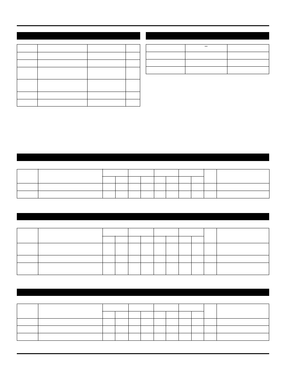
TTL SWITCHING CIRCUIT
PULSE
GENERATOR
IN
OUT
V
EE
V
CC
DEVICE
UNDER
TEST
CH A
OSCILLOSCOPE
CH B
50
COAX
450
Use 0.1µF Capacitors
For Decoupling
Use Oscilloscope Internal
50
Load For Termination
50
COAX
50
COAX

4
SY100ELT25
Micrel
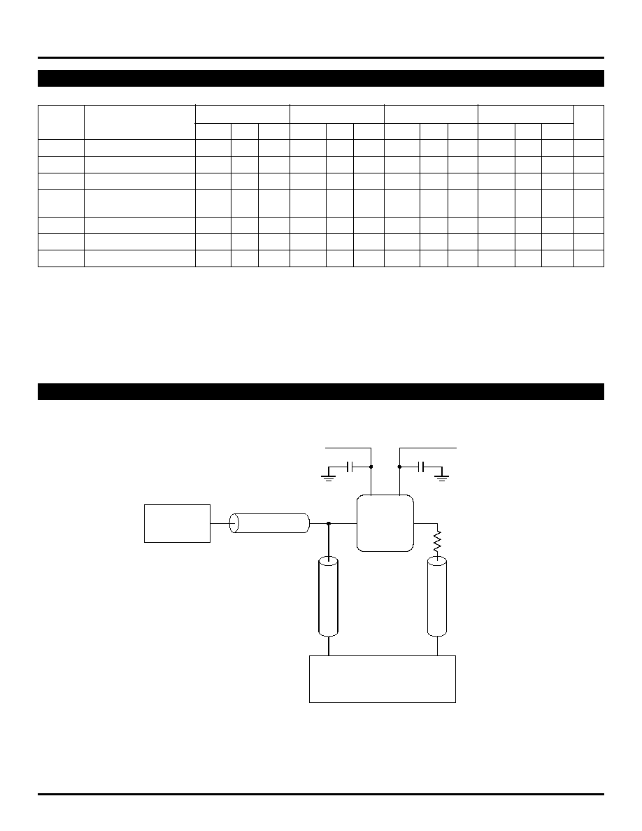
ECL/TTL PROPAGATION DELAY -- SINGLE ENDED
ECL/TTL WAVEFORMS: RISE AND FALL TIMES
PRODUCT ORDERING CODE
Ordering
Package
Operating
Code
Type
Range
SY100ELT25ZC
Z8-1
Commercial
SY100ELT25ZCTR
Z8-1
Commercial
V
IN
V
OUT
50%
1.5V
t
PLH
t
PHL
V
OUT
t
r
t
f
2.0V
1V
5
SY100ELT25
Micrel
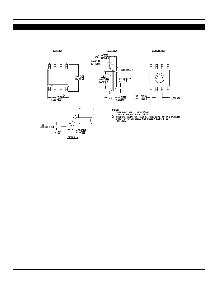
8 LEAD SOIC .150" WIDE (Z8-1)
Rev. 03
MICREL-SYNERGY
3250 SCOTT BOULEVARD
SANTA CLARA
CA 95054
USA
TEL
+ 1 (408) 980-9191
FAX
+ 1 (408) 914-7878
WEB
http://www.micrel.com
This information is believed to be accurate and reliable, however no responsibility is assumed by Micrel for its use nor for any infringement of patents or
other rights of third parties resulting from its use. No license is granted by implication or otherwise under any patent or patent right of Micrel Inc.
© 2000 Micrel Incorporated