DESCRIPTION
s
Up to 1.25Gbps operation
s
25mA peak drive current
s
Adjustable output current
s
Separate output enable
s
Differential inputs for data
s
75K
input pulldown resistor
s
Single power supply
s
Available in a tiny 10-pin (3mm) MSOP
The SY100ELT982 is a high speed PECL-to-CML
translator. The output current is DC current controlled by
I
RSET
, current through the resistor R
SET
. The output OUT
is LOW when output enable is HIGH.
The device incorporates complementary open collector
outputs with a capability of driving peak current of 25mA.
The SY100ELT982 utilizes the high performance
bipolar ASSETTM technology.
FEATURES
PECL-TO-CML
TRANSLATOR
w/o ENABLE
PIN CONFIGURATIONS
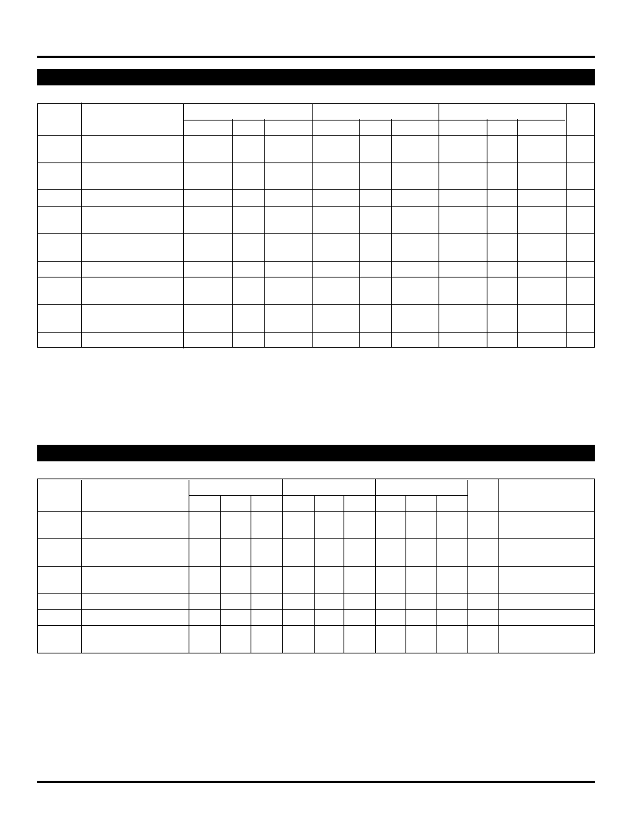
BLOCK DIAGRAM
PRELIMINARY
SY100ELT982
s
Telecommunications
s
CML Output Oscillator
s
GaAS Interface
APPLICATIONS
D
IN
V
CC
R
TERM
OUT
D
IN
Output Current
Control
Internal Logic
BIAS
Control
EN
I
OUT
V
REF
40X
R
SET
V
EE
V
CC
GND
R
SET
OUT
6
5
10
9
8
7
1
2
3
4
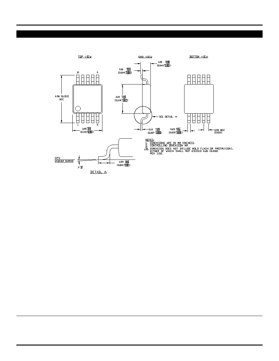
MSOP
K10-1
/EN
D
IN
/D
IN
V
REF
V
CC
/OUT
OUT
GND
GND
R
SET
1
Rev.: A
Amendment: /1
Issue Date:
July 2000
2
PRELIMINARY
SY100ELT982
Micrel
Pin
Function
V
CC
Most positive power supply input, +5V for PECL
operation.
GND
Ground
D
IN
, /D
IN
Differential PECL 100K compatible inputs.
/EN
This PECL 100K compatible input enables data
translation. When Enable asserted HIGH,
OUT = I
OUT
, /OUT = 0mA.
OUT, /OUT
Open collector outputs from the output
buffer drive these differential current outputs.
V
REF
Voltage reference for use with R
SET.
R
SET
External resistor to adjust output current.
D
/D
/EN
OUT
(2)
/OUT
(3)
L
H
L
L
H
H
L
L
H
L
X
X
H
L
H
NOTE:
1. L = LOW, H = HIGH, X = don't care
2. H = I
OUT
= 0mA
3. H = /I
OUT
= 0mA
PIN NAMES
TRUTH TABLE
(1)
Symbol
Rating
Value
Unit
V
CC
Power Supply Voltage
0 to +7.0
V
V
I
Input Voltage
0 to +6.0
V
I
O
Output Current
25
mA
T
A
Operating Temperature Range
0∞C to +85∞C
∞C
T
store
Storage Temperature Range
≠55∞C to +125∞C
∞C
P
tot
Power Dissipation
250
mW
ABSOLUTE MAXIMUM RATINGS
(1)
NOTE:
1. Permanent device damage may occur if ABSOLUTE MAXIMUM RATINGS are exceeded. This is a stress rating only and functional operation is not implied
at conditions other than those detailed in the operational sections of this data sheet. Exposure to ABSOLUTE MAXIMUM RATlNG conditions for extended
periods may affect device reliability.
Symbol
Rating
Value
Unit
V
CC
Power Supply Voltage
+4.5 to +5.5
V
R
TERM
Resistor to Terminate Outputs
10 to 50
R
SET
Resistor to Adjust Current
1500 to 50,000
JA
Thermal Resistance of Package to Ambient
(2)
206
∞C/W
C
OUT
Capacitance on OUT + /OUT
2.5 typical
pf
OPERATIONING CONDITIONS
(1)
NOTES:
1. The voltage drop across R
TERM
should not be greater than 2V.
2. Still air without heatsink.
5
PRELIMINARY
SY100ELT982
Micrel
10 LEAD MSOP (K10-1)
Rev. 00
MICREL-SYNERGY
3250 SCOTT BOULEVARD
SANTA CLARA
CA 95054
USA
TEL
+ 1 (408) 980-9191
FAX
+ 1 (408) 914-7878
WEB
http://www.micrel.com
This information is believed to be accurate and reliable, however no responsibility is assumed by Micrel for its use nor for any infringement of patents or
other rights of third parties resulting from its use. No license is granted by implication or otherwise under any patent or patent right of Micrel Inc.
© 2000 Micrel Incorporated