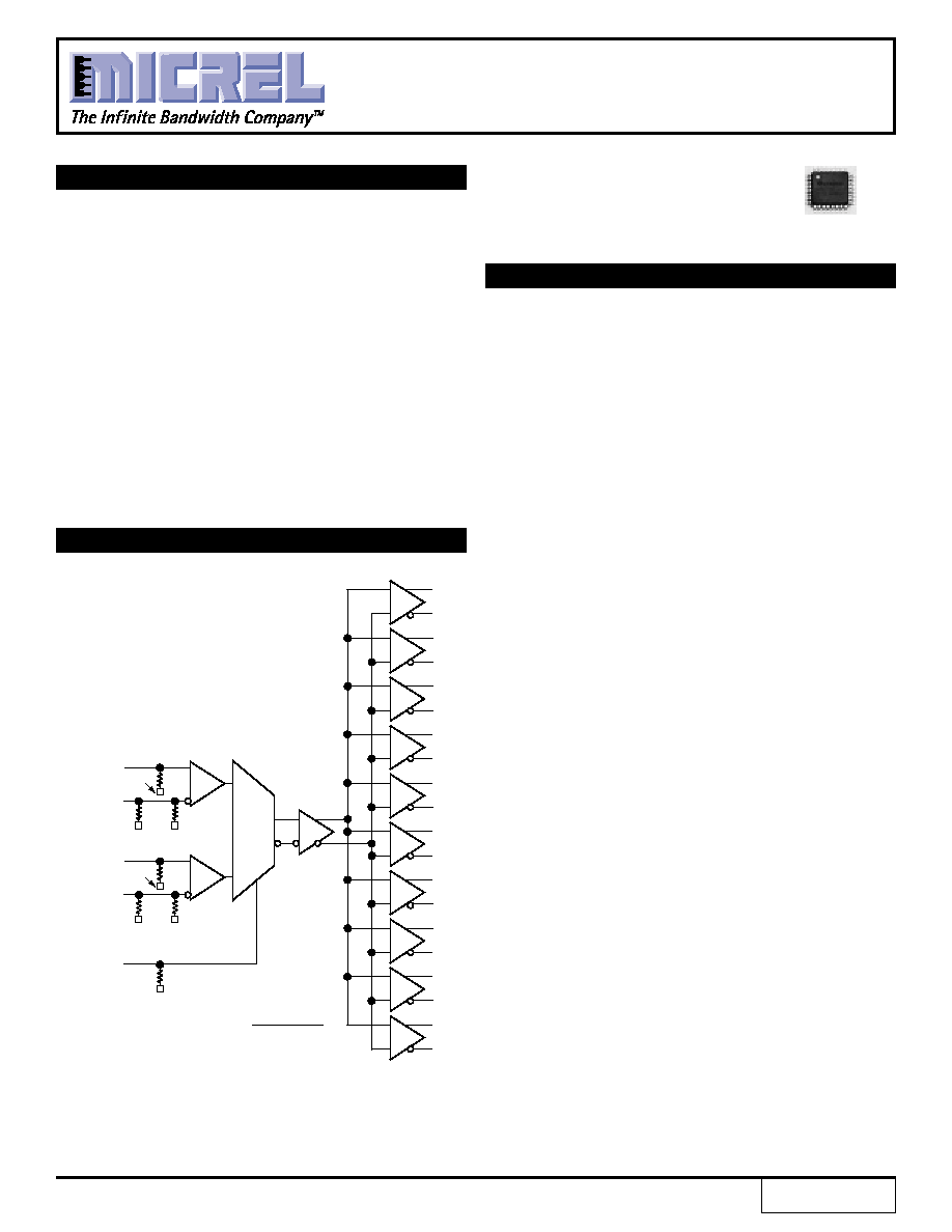
BLOCK DIAGRAM
0
1
CLK0
/CLK0
CLK_SEL
Q
0
/Q
0
Q
1
/Q
1
Q
2
/Q
2
Q
3
/Q
3
Q
4
/Q
4
Q
5
/Q
5
Q
6
/Q
6
Q
7
/Q
7
Q
8
/Q
8
Q
9
/Q
9
V
BB
V
CC
V
EE
CLK1
/CLK1
V
CC
V
EE
V
EE
V
EE
V
EE
75k
75k
75k
75k
75k
75k
75k
FEATURES
s
2.5V and 3.3V power supply options
s
Guaranteed AC parameters over temperature:
∑ f
MAX
= 3GHz
∑ < 25ps output-to-output skew
∑ < 250ps t
r
/ t
f
∑ < 400ps propagation delay
s
Wide temperature range: ≠40
∞
C to +85
∞
C
s
Differential design
s
V
BB
output for single-ended input applications
s
Fully compatible with industry standard 100K I/O
levels
s
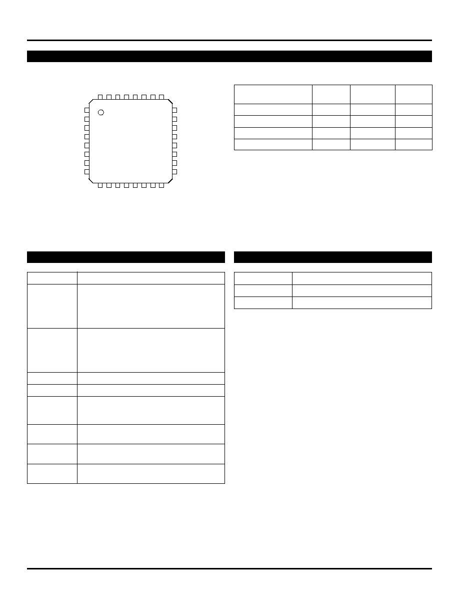
Available in 32-pin TQFP package
The SY100EP111U is a high-speed, low skew 1-to-10
differential fanout buffer designed for clock distribution in
new, high-performance systems. The internal 2:1 mux
allows the input to select between two differential clock
sources.
The device is specifically designed for low skew. The
interconnect scheme and metal layout are carefully
optimized for minimal gate-to-gate skew within the device.
Wafer characterization and process control ensure
consistent distribution of propagation delay from lot to lot.
The V
BB
output is intended for use as a reference
voltage for single-ended reception of ECL signals to that
device only. When using V
BB
for this purpose, it is
recommended that V
BB
is decoupled to V
CC
via a 0.01
µ
F
capacitor.
2.5V/3.3V 1:10 DIFFERENTIAL
LVPECL/LVECL/HSTL
CLOCK DRIVER
DESCRIPTION
Precision EdgeTM
SY100EP111U
FINAL
1
Rev.: D
Amendment: /0
Issue Date:
March 2003
Precision Edge is a trademark of Micrel, Inc.
Precision EdgeTM
2
Precision EdgeTM
SY100EP111U
Micrel
PACKAGE/ORDERING INFORMATION
Ordering Information
Package
Operating
Package
Part Number
Type
Range
Marking
SY100EP111UTC
T32-1
Commercial
XEP111U
SY100EP111UTCTR
(1)
T32-1
Commercial
XEP111U
SY100EP111UTI
(2)
T32-1
Industrial
XEP111U
SY100EP111UTITR
(1,2)
T32-1
Industrial
XEP111U
Note 1.
Tape and Reel
Note 2.
Recommended for new designs.
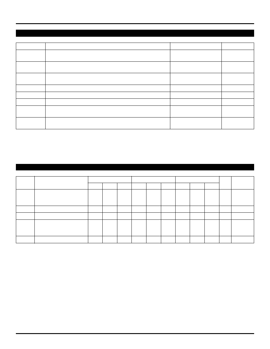
32 31 30 29 28 27 26 25
9
10 11 12 13 14 15 16
1
2
3
4
5
6
7
8
24
23
22
21
20
19
18
17
VCC
CLK_SEL
CLK0
/CLK0
VBB
CLK1
/CLK1
VEE
Q3
/Q3
Q4
/Q4
Q5
/Q5
Q6
/Q6
VCC
Q0
/Q0
Q1
/Q1
Q2
/Q2
VCC
VCC
/Q9
Q9
/Q8
Q8
/Q7
Top View
TQFP
T32-1
Q7
VCC
32-Pin TQFP (T32-1)
Pin
Function
CLK0, /CLK0
LVPECL, LVECL, HSTL Clock Inputs:
CLK0 input includes a 75k
pull-down. Default
is low if left floating. /CLK0 includes an internal
75k
pull-up and pull-down. Default state is
V
CC
/2.
CLK1, /CLK1
LVPECL, LVECL, HSTL Clock Inputs:
CLK input includes a 75k
pull-down. Default
is low if left floating. /CLK includes an internal
75k
pull-up and pull-down. Default state is
V
CC
/2.
Q0 to Q9
LVPECL/LVECL Outputs.
/Q0 to /Q9
Complementary LVPECL/LVECL Outputs.
CLK_SEL
LVPECL/LVECL Clock Select Input: Internal
75k
resistor connected to V
EE
. When left
floating, the default condition is LOW.
V
BB
Reference Voltage: AC coupled or single-
ended input applications.
V
CC
Positive Power Supply: Bypass with 0.1
µ
F//
0.01
µ
F low ESR capacitors.
V
EE
Negative Power Supply: LVPECL operation,
connect to GND.
PIN NAMES
CLK_SEL
Active Input
0
CLK0, /CLK0
1
CLK1, /CLK1
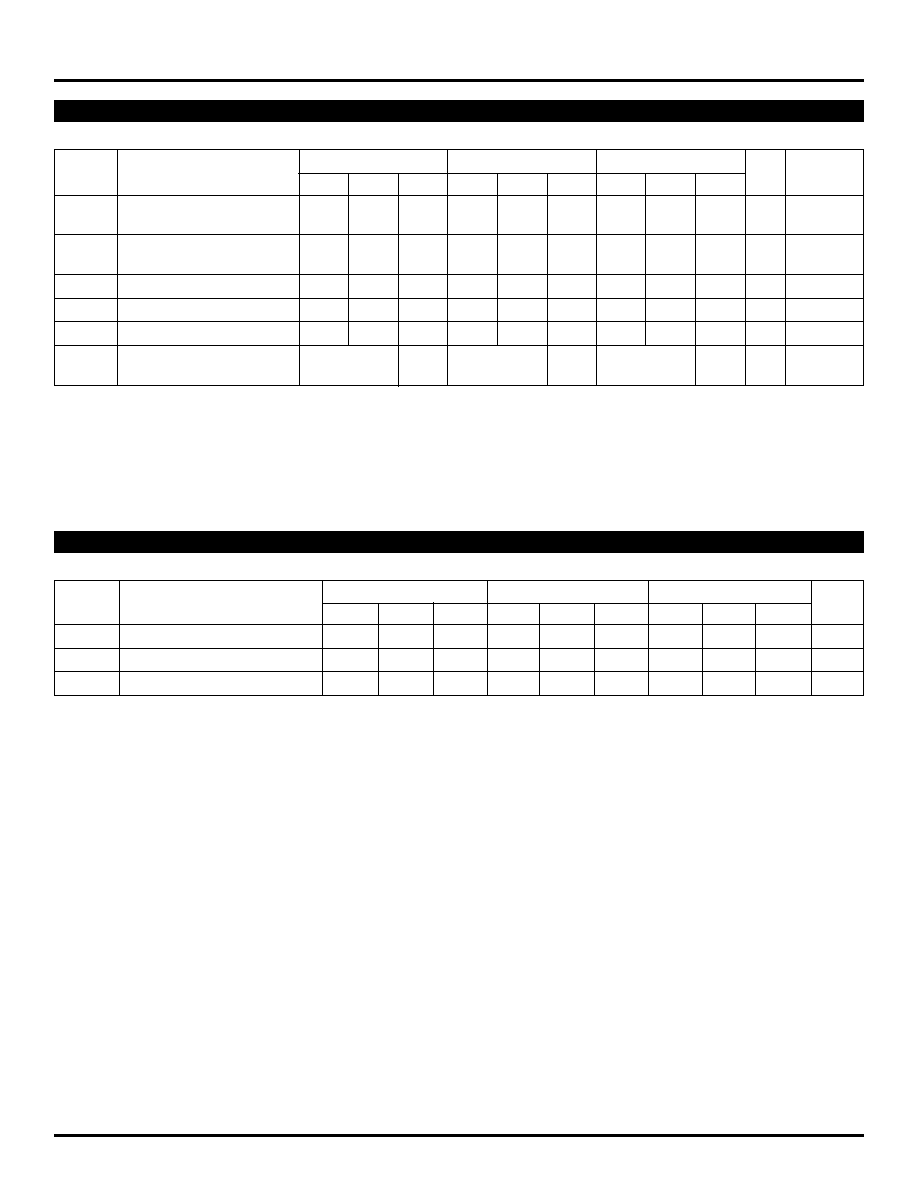
FUNCTION TABLE
3
Precision EdgeTM
SY100EP111U
Micrel
Symbol
Rating
Value
Unit
V
CC
≠ V
EE
Power Supply Voltage
6.0
V
V
IN
Input Voltage (V
CC
= 0V, V
IN
not more negative than V
EE
)
≠6.0 to 0
V
Input Voltage (V
EE
= 0V, V
IN
not more positive than V
CC
)
+6.0 to 0
I
OUT
Output Current
≠Continuous
50
mA
≠Surge
100
I
BB
V
BB
Sink/Source Current
(2)
±
0.5
mA
T
A
Operating Temperature Range
≠40 to +85
∞
C
T
store
Storage Temperature Range
≠65 to +150
∞
C
JA
Package Thermal Resistance
≠Still-Air
50
∞
C/W
(Junction-to-Ambient)
≠500lfpm
42
JC
Package Thermal Resistance
20
∞
C/W
(Junction-to-Case)
ABSOLUTE MAXIMUM RATINGS
(1)
Note 1.
Permanent device damage may occur if ABSOLUTE MAXIMUM RATINGS are exceeded. This is a stress rating only and functional operation
is not implied at conditions other than those detailed in the operational sections of this data sheet. Exposure to ABSOLUTE MAXIMUM
RATlNG conditions for extended periods may affect device reliability.
Note 2.
Due to the limited drive capability, use for inputs of same package only.
T
A
= ≠40
∞
C
T
A
= +25
∞
C
T
A
= +85
∞
C
Symbol
Parameter
Min.
Typ.
Max.
Min.
Typ.
Max.
Min.
Typ.
Max.
Unit
Condition
V
CC
Power Supply Voltage
(LVPECL)
2.375
--
3.8
2.375
--
3.8
2.375
--
3.8
V
(LVECL)
≠3.8
--
≠2.375
≠3.8
--
≠2.375
≠3.8
--
≠2.375
V
I
EE
Power Supply Current
--
55
120
--
70
120
--
85
120
mA
I
IH
Input HIGH Current
--
--
150
--
--
150
--
--
150
µ
A
V
IN
= V
IH
I
IL
Input LOW Current
CLK0, CLK1
0.5
--
--
0.5
--
--
0.5
--
--
µ
A
V
IN
= V
IL
/CLK0, /CLK1
≠150
--
--
≠150
--
--
≠150
--
--
µ
A
V
IN
= V
IL
C
IN
Input Capacitance
--
--
--
--
2
--
--
--
--
pF
Note 1.
100KEP circuits are designed to meet the DC specifications shown in the above table after thermal equilibrium has been established. The
circuit is in a test socket or mounted on a printed circuit board and traverse airflow greater than 500lfpm is maintained.
DC ELECTRICAL CHARACTERISTICS
(1)
4
Precision EdgeTM
SY100EP111U
Micrel
T
A
= ≠40
∞
C
T
A
= +25
∞
C
T
A
= +85
∞
C
Symbol
Parameter
Min.
Typ.
Max.
Min.
Typ.
Max.
Min.
Typ.
Max.
Unit
Condition
V
IH
Input HIGH Voltage
2135
--
2420
2135
--
2420
2135
--
2420
mV
(Single-Ended)
V
IL
Input LOW Voltage
1355
--
1675
1355
--
1675
1355
--
1675
mV
(Single-Ended)
V
OL
Output LOW Voltage
1355
1480
1605
1355
1480
1605
1355
1480
1605
mV
50
to V
CC
≠2V
V
OH
Output HIGH Voltage
2155
2280
2405
2155
2280
2405
2155
2280
2405
mV
50
to V
CC
≠2V
V
BB
Reference Voltage
(2)
1775
1875
1975
1775
1875
1975
1775
1875
1975
mV
V
IHCMR
Input HIGH Voltage
1.2
--
V
CC
1.2
--
V
CC
1.2
--
V
CC
V
Common Mode Range
(3)
LVPECL DC ELECTRICAL CHARACTERISTICS
(1)
V
CC
= 3.3V
±
10%; V
EE
= 0V
Note 1.
100KEP circuits are designed to meet the DC specifications shown in the above table after thermal equilibrium has been established. The
circuit is in a test socket or mounted on a printed circuit board and traverse airflow greater than 500lfpm is maintained. Input and output varies
1:1 with V
CC
.
Note 2.
Single-ended input operation is limited V
CC
3.0V in LVPECL mode. V
BB
reference varies 1:1 with V
CC
.
Note 3.
V
IHCMR
(Min) varies 1:1 with V
EE
, V
IHCMR
(Max) varies 1:1 with V
CC
. The V
IHCMR
range is referenced to the most positive side of the
differential input signal.
T
A
= ≠40
∞
C
T
A
= +25
∞
C
T
A
= +85
∞
C
Symbol
Parameter
Min.
Typ.
Max.
Min.
Typ.
Max.
Min.
Typ.
Max.
Unit
Condition
V
IH
Input HIGH Voltage
1335
--
1620
1335
--
1620
1335
--
1620
mV
(Single-ended)
V
IL
Input LOW Voltage
555
--
875
555
--
875
555
--
875
mV
(Single-ended)
V
OL
Output LOW Voltage
555
680
805
555
680
805
555
680
805
mV
50
to V
CC
≠2V
V
OH
Output HIGH Voltage
1355
1480
1605
1355
1480
1605
1355
1480
1605
mV
50
to V
CC
≠2V
V
IHCMR
Input HIGH Voltage
1.2
--
V
CC
1.2
--
V
CC
1.2
--
V
CC
V
Common Mode Range
(2)
Note 1.
100KEP circuits are designed to meet the DC specifications shown in the above table after thermal equilibrium has been established. The
circuit is in a test socket or mounted on a printed circuit board and traverse airflow greater than 500lfpm is maintained. Input and output varies
1:1 with V
CC
.
Note 2.
V
IHCMR
(Min) varies 1:1 with V
EE
, V
IHCMR
(Max) varies 1:1 with V
CC
. The V
IHCMR
range is referenced to the most positive side of the differen-
tial input signal.
LVPECL DC ELECTRICAL CHARACTERISTICS
(1)
V
CC
= 2.5V
±
5%, V
EE
= 0V
5
Precision EdgeTM
SY100EP111U
Micrel
T
A
= ≠40
∞
C
T
A
= +25
∞
C
T
A
= +85
∞
C
Symbol
Parameter
Min.
Typ.
Max.
Min.
Typ.
Max.
Min.
Typ.
Max.
Unit
V
IH
Input HIGH Voltage
1200
--
--
1200
--
--
1200
--
--
mV
V
IL
Input LOW Voltage
--
--
400
--
--
400
--
--
400
mV
V
X
Input Crossover Voltage
680
--
900
680
--
900
680
--
900
mV
HSTL DC ELECTRICAL CHARACTERISTICS
V
CC
= 2.375V to 3.8V; V
EE
= 0V
T
A
= ≠40
∞
C
T
A
= +25
∞
C
T
A
= +85
∞
C
Symbol
Parameter
Min.
Typ.
Max.
Min.
Typ.
Max.
Min.
Typ.
Max.
Unit
Condition
V
IL
Input LOW Voltage
≠1945
--
≠1625 ≠1945
--
≠1625 ≠1945
--
≠1625
mV
(Single-ended)
V
IH
Input HIGH Voltage
≠1165
--
≠0880 ≠1165
--
≠0880 ≠1165
--
≠0880
mV
(Single-ended)
V
OL
Output LOW Voltage
≠1945 ≠1820 ≠1695 ≠1945 ≠1820 ≠1695 ≠1945 ≠1820 ≠1695
mV
50
to V
CC
≠2V
V
OH
Output HIGH Voltage
≠1145 ≠1020 ≠0895 ≠1145 ≠1020 ≠0895 ≠1145 ≠1020 ≠0895
mV
50
to V
CC
≠2V
V
BB
Output Reference Voltage
(2)
≠1525 ≠1425 ≠1325 ≠1525 ≠1425 ≠1325 ≠1525 ≠1425 ≠1325
mV
V
IHCMR
Input HIGH Voltage
V
EE
+1.2
0.0
V
EE
+1.2
0.0
V
EE
+1.2
0.0
V
Common Mode Range
(3)
Note 1.
100KEP circuits are designed to meet the DC specifications shown in the above table after thermal equilibrium has been established. The
circuit is in a test socket or mounted on a printed circuit board and traverse airflow greater than 500lfpm is maintained.
Note 2.
Single-ended input operation is limited V
EE
≠3.0V in LVECL mode.
Note 3.
V
IHCMR
(min) varies 1:1 with V
EE
. The V
IHCMR
range is referenced to the most positive side of the differential input signal.
LVECL DC ELECTRICAL CHARACTERISTICS
(1)
V
EE
= ≠2.375V to ≠3.8V; V
CC
= 0V