1
ECL ProTM
SY100EP15V
Micrel, Inc.
M9999-120505
hbwhelp@micrel.com or (408) 955-1690
The SY100EP15V is a high-speed, low-skew, PECL/ECL
1:4 precision fanout buffer with a 2:1 mux front end in a
small 16-pin TSSOP package. The 2:1 mux input accepts a
single-ended PECL/ECL source (CLK1) and a differential
PECL/ECL/HSTL source (CLK0). All I/O pins are 100K EP
PECL/ECL logic compatible.
AC performance is guaranteed over the industrial ≠40∞C
to +85∞C temperature range and 3.3V to 5V supply voltage.
This device will operate in PECL/LVPECL or ECL/LVECL
mode. For clock applications, the high-speed design
combined with an extremely fast rise/fall time of less than
225ps produces a toggle frequency as high as 2.5GHz
(~400mV
PP
swing).
A V
BB
output reference pin is available for AC≠coupled
and single-ended input applications. In addition, a
synchronous output enable function is provided.
The SY100EP15V is part of Micrel's high-speed, precision
edge timing and distribution family. For applications that
require a different I/O combination, consult Micrel's website
at www.micrel.com, and choose from a comprehensive
product line of high-speed, low-skew fanout buffers,
translators, and clock dividers.
All support documentation can be found on Micrel's web
site at: www.micrel.com.
FEATURES
DESCRIPTION
Rev.: E
Amendment: /0
Issue Date:
December 2005
ECL ProTM
SY100EP15V
High-speed 1:4 PECL/ECL fanout buffer
2:1 multiplexer input
Guaranteed AC parameters over temp/voltage:
∑ > 2.5GHz f
MAX
(toggle)
∑ < 225ps rise/fall times
∑ < 25ps within device skew
∑ < 425ps propagation delay (CLK-to-Q)
Low jitter design:
∑ < 1ps
RMS
cycle-to-cycle jitter
∑ < 20ps
PP
total jitter
Flexible power supply: 3.3V/5V
Wide operating temperature range: ≠40
∞
C to +85
∞
C
V
BB
reference for AC-coupled or single-ended
applications
Output enable/disable function
100K PECL/ECL compatible logic
Input accepts PECL/LVPECL/ECL/HSTL logic levels
Available in a 16-pin TSSOP package
3.3V/5V 2.5GHz PECL/ECL
1:4 FANOUT BUFFER
WITH 2:1 INPUT MUX
ECL ProTM
ECL Pro is a trademark of Micrel, Inc.
2
ECL ProTM
SY100EP15V
Micrel, Inc.
M9999-120505
hbwhelp@micrel.com or (408) 955-1690
PACKAGE/ORDERING INFORMATION
Ordering Information
(1)
Package
Operating
Package
Lead
Part Number
Type
Range
Marking
Finish
SY100EP15VK4C
K4-16-1
Commercial
XEP15V
Sn-Pb
SY100EP15VK4CTR
(2)
K4-16-1
Commercial
XEP15V
Sn-Pb
SY100EP15VK4I
K4-16-1
Industrial
XEP15V
Sn-Pb
SY100EP15VK4ITR
(2)
K4-16-1
Industrial
XEP15V
Sn-Pb
SY100EP15VK4G
(3)
K4-16-1
Industrial
XEP15V with
NiPdAu
Pb-Free bar-line Indicator
Pb-Free
SY100EP15VK4GTR
(2, 3)
K4-16-1
Industrial
XEP15V with
NiPdAu
Pb-Free bar-line Indicator
Pb-Free
Notes:
1. Contact factory for die availability. Dice are guaranteed at T
A
= 25∞C, DC Electricals only.
2. Tape and Reel.
3. Pb-Free package is recommended for new designs.
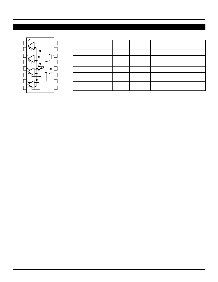
Available in 16-Pin TSSOP
(K4-16-1)
1
Q0
/Q0
Q1
/Q1
Q2
/Q2
Q3
/Q3
16 VCC
/EN
CLK1
VBB
/CLK0
CLK0
SEL
VEE
2
15
3
14
4
13
5
12
6
11
7
10
8
9
D
Q
1
0
3
ECL ProTM
SY100EP15V
Micrel, Inc.
M9999-120505
hbwhelp@micrel.com or (408) 955-1690
TRUTH TABLE
(1)
CLK0
CLK1
SEL
/EN
Q
L
X
L
L
L
H
X
L
L
H
X
L
H
L
L
X
H
H
L
H
X
L
H
L
X
H
H
L
PIN DESCRIPTION
Pin
Pin Number
Function
1, 2, 3, 4
Q0 ≠ Q3
Outputs 0 through 3: 100KEP (LV)PECL/(LV)ECL compatible differential outputs. Terminate
5, 6, 7, 8
/Q0 ≠ /Q3
with 50 to V
CC
≠2V. Unused output pairs may be left floating, or pulled-down with a 2k
resistor to the most negative supply. Unused single-ended outputs must have a balanced load.
For AC-coupled applications, the output stage emitter follower must have a DC current path to
ground. See "Termination" section.
9
VEE
Negative Power Supply: For PECL/LVPECL applications, connect to GND.
10
SEL
100KEP (LV)PECL/(LV)ECL Compatible 2:1 Mux Input Select Control. See "Truth Table." The
select (SEL) pin includes an internal 75k pull-down resistor. Default condition when left floating
is LOW, and CLK0 input is selected.
11, 12
CLK0, /CLK0
Differential (LV)PECL/(LV)ECL/HSTL Compatible Input: The inputs include an internal 75k
pull-down resistor on CLK0 and internal 75k pull-up and pull-down on /CLK0. Default condition
for CLK0 is LOW when left floating and V
CC
/2 for /CLK0 when left floating.
13
VBB
Reference Output Voltage: This reference is typically used to bias the unused inverting input for
single-ended input applications, or as the termination point for AC-coupled differential input
applications. V
BB
reference value is approximately V
CC
≠1.3V, and tracks Vcc 1:1. Maximum
sink/source capability for V
BB
is 0.50mA. For single ended inputs, connect to the unused input
through a 50 resistor. Decouple the V
BB
pin with a 0.01µF capacitor to V
CC
.
14
CLK1
Single-Ended (LV)PECL/(LV)ECL Compatible Input: This pin includes an internal 75k
pull-down resistor. Default condition is LOW when left floating.
15
/EN
100KEP (LV)PECL/(LV)ECL Compatible Input: This synchronous pin controls the output state.
See "Truth Table." To ensure proper synchronous operation, adhere to the Set-up and Hold
times, as described in the AC electrical table. When /EN pin goes HIGH, Q outputs go LOW, and
/Q outputs go HIGH on the next falling clock transition. This synchronous operation avoids any
chance of generating a runt pulse.
16
VCC
Positive Power Supply: Bypass with 0.1µF//0.01µF low ESR capacitors.
Note:
1.
= Negative edge.
4
ECL ProTM
SY100EP15V
Micrel, Inc.
M9999-120505
hbwhelp@micrel.com or (408) 955-1690
Symbol
Rating
Value
Unit
V
CC
≠ V
EE
Power Supply Voltage
6.0
V
V
IN
Input Voltage (V
CC
= 0V, V
IN
not more negative than V
EE
)
≠6.0 to 0
V
Input Voltage (V
EE
= 0V, V
IN
not more positive than V
CC
)
+6.0 to 0
I
OUT
Output Current
≠Continuous
50
mA
≠Surge
100
I
BB
V
BB
Sink/Source Current
(2)
±0.5
mA
T
LEAD
Lead Temperature (soldering, 20sec.)
+260
∞C
T
A
Operating Temperature Range
≠40 to +85
∞C
T
STORE
Storage Temperature Range
≠65 to +150
∞C
JA
Package Thermal Resistance
≠Still-Air (single-layer PCB)
115
(Junction-to-Ambient)
≠Still-Air (multi-layer PCB)
75
∞C/W
≠500lfpm (multi-layer PCB)
65
JC
Package Thermal Resistance
21
∞C/W
(Junction-to-Case)
Notes:
1. Permanent device damage may occur if absolute maximum ratings are exceeded. This is a stress rating only and functional operation is not implied
at conditions other than those detailed in the operational sections of this data sheet. Exposure to absolute maximum ratlng conditions for extended
periods may affect device reliability.
2. Due to the limited drive capability, use for inputs of same package only.
ABSOLUTE MAXIMUM RATINGS
(1)
T
A
= ≠40
∞
C
T
A
= +25
∞
C
T
A
= +85
∞
C
Symbol
Parameter
Min.
Typ.
Max.
Min.
Typ.
Max.
Min.
Typ.
Max.
Unit
Condition
V
CC
Power Supply Voltage
V
(PECL)
4.5
5.0
5.5
4.5
5.0
5.5
4.5
5.0
5.5
(LVPECL)
2.97
3.3
3.63
2.97
3.3
3.63
2.97
3.3
3.63
(ECL)
≠5.5
≠5.0
≠4.5
≠5.5
≠5.0
≠4.5
≠5.5
≠5.0
≠4.5
(LVECL)
≠3.63
≠3.3
≠2.97
≠3.63
≠3.3
≠2.97
≠3.63
≠3.3
≠2.97
I
CC
Power Supply Current
--
--
70
--
52
72
--
--
75
mA
I
IH
Input HIGH Current
--
--
150
--
--
150
--
--
150
µA
V
IN
= V
IH
I
IL
Input LOW Current
CLK0, CLK1
0.5
--
--
0.5
--
--
0.5
--
--
µA
V
IN
= V
IL
/CLK0
≠150
--
--
≠150
--
--
≠150
--
--
µA
V
IN
= V
IL
C
IN
Input Capacitance (TSSOP)
--
--
--
--
1.0
--
--
--
--
pF
Note:
1. 100KEP circuits are designed to meet the DC specifications shown in the above table after thermal equilibrium has been established. The circuit is in
a test socket or mounted on a printed circuit board and traverse airflow greater than 500lfpm is maintained.
DC ELECTRICAL CHARACTERISTICS
(1)

5
ECL ProTM
SY100EP15V
Micrel, Inc.
M9999-120505
hbwhelp@micrel.com or (408) 955-1690
T
A
= ≠40
∞
C
T
A
= +25
∞
C
T
A
= +85
∞
C
Symbol
Parameter
Min.
Typ.
Max.
Min.
Typ.
Max.
Min.
Typ.
Max.
Unit
Condition
V
IL
Input LOW Voltage
1355
--
1675
1355
--
1675
1355
--
1675
mV
V
CC
= 3.3V
(Single-Ended)
V
IH
Input HIGH Voltage
2075
--
2420
2075
--
2420
2075
--
2420
mV
V
CC
= 3.3V
(Single-Ended)
V
OL
Output LOW Voltage
1355
1480
1605
1355
1480
1605
1355
1480
1605
mV
V
CC
= 3.3V
V
OH
Output HIGH Voltage
2155
2280
2405
2155
2280
2405
2155
2280
2405
mV
V
CC
= 3.3V
V
BB
Reference Voltage
(2)
1775
1875
1975
1775
1875
1975
1775
1875
1975
mV
V
CC
= 3.3V
V
IHCMR
Input HIGH Voltage
1.2
--
V
CC
1.2
--
V
CC
1.2
--
V
CC
V
Common Mode Range
(3)
Notes:
1. 100KEP circuits are designed to meet the DC specifications shown in the above table after thermal equilibrium has been established. The circuit is in
a test socket or mounted on a printed circuit board and traverse airflow greater than 500lfpm is maintained. Input and output parameters varies 1:1
with V
CC
. Output load is 50 to V
CC
≠2V.
2. V
BB
varies 1:1 with V
CC
.
3. The V
IHCMR
range is referenced to the most positive side of the differential input signal.
(100KEP) LVPECL DC ELECTRICAL CHARACTERISTICS
(1)
V
CC
= 3.0V ±10%, V
EE
= 0V
T
A
= ≠40
∞
C
T
A
= +25
∞
C
T
A
= +85
∞
C
Symbol
Parameter
Min.
Typ.
Max.
Min.
Typ.
Max.
Min.
Typ.
Max.
Unit
Condition
V
IL
Input LOW Voltage
3055
--
3375
3055
--
3375
3055
--
3375
mV
V
CC
= 5V
(Single-Ended)
V
IH
Input HIGH Voltage
3775
--
4120
3775
--
4120
3775
--
4120
mV
V
CC
= 5V
(Single-Ended)
V
OL
Output LOW Voltage
3055
3180
3305
3055
3180
3305
3055
3180
3305
mV
V
CC
= 5V
V
OH
Output HIGH Voltage
3855
3980
4105
3855
3980
4105
3855
3980
4105
mV
V
CC
= 5V
V
BB
Output Voltage Reference
(2)
3475
3575
3675
3475
3575
3675
3475
3575
3675
mV
V
CC
= 5V
V
IHCMR
Input HIGH Voltage
(3)
1.2
--
V
CC
1.2
--
V
CC
1.2
--
V
CC
V
Common Mode Range
Notes:
1. 100KEP circuits are designed to meet the DC specifications shown in the above table after thermal equilibrium has been established. The circuit is in
a test socket or mounted on a printed circuit board and traverse airflow greater than 500lfpm is maintained. Input and output parameters varies 1:1
with V
CC
. Output load is 50 to V
CC
≠2V.
2. V
BB
varies 1:1 with V
CC
.
3. The V
IHCMR
range is referenced to the most positive side of the differential input signal.
(100KEP) PECL DC ELECTRICAL CHARACTERISTICS
(1)
V
CC
= 5.0V ±10%, V
EE
= 0V