1
ECL ProTM
SY100EP16VS
Micrel
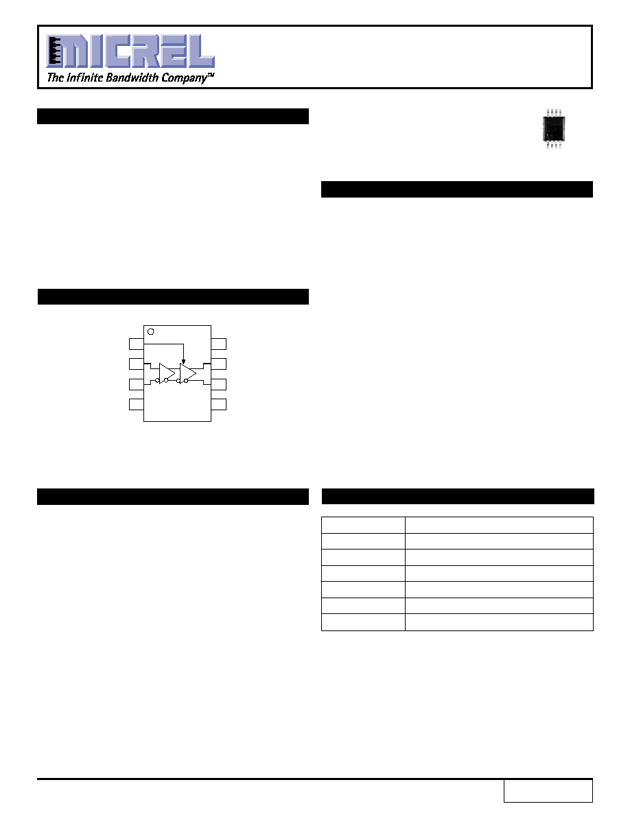
Pin
Function
D, /D
PECL Data Inputs
Q, /Q
Data Outputs
V
BB
Reference Voltage Output
V
CTRL
Output Swing Control
V
CC
Most Positive Power Supply Input
V
EE
Most Negative Power Supply Input
DESCRIPTION
FEATURES
5V/3.3V 2.5Gbps
VARIABLE OUTPUT SWING
DIFFERENTIAL RECEIVER
ECL ProTM
SY100EP16VS
FINAL
s
3.3V and 5V power supply options
s
Fast output transitions <160ps t
r
/ t
f
s
Guaranteed operation over ≠40
∞
C to +85
∞
C
temperature range
s
Functionally equivalent to SY88927V and
SY10EP16V
s
Variable output swing from 100mV to 700mV
s
Available in 8-pin (3mm) EPAD-MSOP package
The SY100EP16VS are differential receivers with
variable output swing. The devices are functionally
equivalent to the EP16V devices with an input that
controls the amplitude of the outputs. EP16VS is
commonly used as VCSEL laser driver.
The operational range of the EP16VS control input is
from V
BB
(max. swing) to V
CC
(min. swing). Simple control
of the output swing can be obtained by a variable resistor
between the V
BB
pin and V
CC
with the wiper driving
V
CTRL
.
The EP16VS provides a V
BB
output for either single-
ended use or as a DC bias for AC coupling to the device.
The V
BB
pin should be used only as a bias for the
EP16VS as its current sink/source capability is limited.
Whenever used, the V
BB
pin should be bypassed to
ground via a 0.01
µ
F capacitor.
Under open input conditions (pulled to V
EE
), internal
input clamps will force the Q output LOW.
PIN NAMES
PIN CONFIGURATION/BLOCK DIAGRAM
Rev.: C
Amendment: /0
Issue Date:
March 2003
1
2
3
4
8
VCC
Q
VEE
D
VBB
/Q
VCTRL
/D
7
6
5
8-pin EPAD-MSOP
APPLICATIONS
s
Multimode optical transceiver
s
VCSEL driver
s
Backplane receiver
ECL ProTM
ECL Pro is a trademark of Micrel, Inc.
2
ECL ProTM
SY100EP16VS
Micrel
Symbol
Rating
Value
Unit
V
EE
Power Supply Voltage (V
CC
= 0)
≠6.0 to 0
V
V
CC
Power Supply Voltage (V
EE
= 0)
+6.0 to 0
V
V
IN
Input Voltage (V
CC
= 0V, V
IN
not more negative than V
EE
)
≠6.0 to 0
V
Input Voltage (V
EE
= 0V, V
IN
not more negative than V
CC
)
+6.0 to 0
V
I
OUT
Output Current
≠Continuous
50
mA
≠Surge
100
I
BB
V
BB
Sink/Source Current
(2)
±
0.5
mA
T
A
Operating Temperature Range
≠40 to +85
∞
C
T
store
Storage Temperature Range
≠65 to +150
∞
C
JA
Package Thermal Resistance
≠Still-Air
38
∞
C/W
(Junction-to-Ambient)
Note 1.
Permanent device damage may occur if ABSOLUTE MAXIMUM RATINGS are exceeded. This is a stress rating only and functional operation
is not implied at conditions other than those detailed in the operational sections of this data sheet. Exposure to ABSOLUTE MAXIMUM
RATlNG conditions for extended periods may affect device reliability.
ABSOLUTE MAXIMUM RATINGS
(1)
T
A
= ≠40
∞
C
T
A
= +25
∞
C
T
A
= +85
∞
C
Symbol
Parameter
Min.
Max.
Min.
Typ.
Max.
Min.
Max.
Unit
I
EE
Power Supply Current
--
51
--
--
51
--
51
mA
V
BB
Output Reference Voltage
V
CC
≠1.38
V
CC
≠1.26
V
CC
≠1.38
--
V
CC
≠1.26
V
CC
≠1.38
V
CC
≠1.26
V
V
OH
Output HIGH Voltage
(3)
V
CC
≠1085
V
CC
≠880
V
CC
≠1025 V
CC
≠0955
V
CC
≠880
V
CC
≠1025
V
CC
≠880
mV
V
OL
Output LOW Voltage
(3)
V
CTRL
= V
BB
V
CC
≠1900 V
CC
≠1650 V
CC
≠1900
--
V
CC
≠1650 V
CC
≠1900 V
CC
≠1650
mV
V
CTRL
= V
CC
V
CC
≠1125
V
CC
≠975
V
CC
≠1125
--
V
CC
≠975
V
CC
≠1125
V
CC
≠975
mV
V
IH
Input HIGH Voltage
V
CC
≠1165
V
CC
≠880
V
CC
≠1165
--
V
CC
≠880
V
CC
≠1165
V
CC
≠880
mV
V
IL
Input LOW Voltage
V
CC
≠1810 V
CC
≠1475 V
CC
≠1810
--
V
CC
≠1475 V
CC
≠1810 V
CC
≠1475
mV
I
IH
Input HIGH Current
D, /D
--
150
--
--
150
--
150
µ
A
V
CTRL
(4)
--
80
--
--
80
--
80
I
IL
Input LOW Current
0.5
--
0.5
--
--
0.5
--
µ
A
Note 1.
100EP circuits are designed to meet the DC specifications shown in the above table after thermal equilibrium has been established. The circuit
is in a test socket or mounted on a printed circuit board and traverse airflow greater than 500lfpm is maintained.
Note 2.
Input and output parameters vary 1:1 with V
CC
.
Note 3.
All loading with 50
to V
CC
≠ 2.0V.
Note 4.
V
CTRL
= V
CC
≠0.88V.
DC ELECTRICAL CHARACTERISTICS
(1)
V
CC
= +5V
±
10% or +3.3V
±
10%; R
LOAD
= 50
to V
CC
≠2V
(2)
3
ECL ProTM
SY100EP16VS
Micrel
Note 1.
Minimum input swing for which AC parameters are guaranteed. The device has a DC gain of
40 when output has a full swing.
Note 2.
The CMR range is referenced to the most positive side of the differential input signal. Normal operation is obtained if the HIGH level falls
within the specified range and the peak-to-peak voltage lies between V
PP
(min.) and 1V. The lower end of the CMR range varies 1:1 with V
EE
.
The numbers in the spec table assume a nominal V
EE
= ≠3.3V and V
CC
= 0V. Note for PECL operation, the V
CMR
(min.) will be fixed at 3.3V
≠ |V
CMR
(min.)|.
Note 3.
Output at full swing.
T
A
= ≠40
∞
C
T
A
= +25
∞
C
T
A
= +85
∞
C
Symbol
Parameter
Min.
Typ.
Max.
Min.
Typ.
Max.
Min.
Typ.
Max.
Unit
t
PLH
Propagation Delay
D (Diff)
100
--
250
100
--
250
120
--
300
ps
t
PHL
to Output
D (SE)
100
250
350
100
250
350
120
280
400
V
PP
Minimum Input Swing
(1)
150
--
--
150
--
--
150
--
--
mV
V
CMR
Common Mode Range
(2)
V
CC
≠1.3
--
V
CC
≠0.4 V
CC
≠1.3
--
V
CC
≠0.4 V
CC
≠1.3
--
V
CC
≠0.4
V
t
r
, t
f
Output Rise/Fall Times
(3)
Q
--
--
160
--
95
160
--
--
160
ps
(20% to 80%)
AC ELECTRICAL CHARACTERISTICS
V
CC
= +5V
±
10% or +3.3V
±
10%; R
LOAD
= 50
to V
CC
≠2V
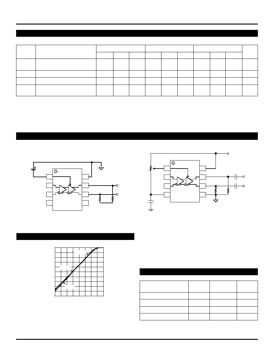
APPLICATION IMPLEMENTATION
8
7
6
5
1
2
3
4
D
/D
Q
/Q
V
SWING
(pk-pk)
≠2V
50
50
V
CC
V
CTRL
V
CTRL
V
BB
V
EE
Figure 1. Voltage Source Implementation
0
10
20
30
40
50
60
70
80
90
100
0 0.2 0.4 0.6 0.8 1.0 1.2 1.4 1.6
VOLTAGE SWING (%)
V
CC
≠ V
CTRL
-40
∞
C
+45
∞
C
+105
∞
C
Figure 3. Typical Voltage Output Swing
V
CC
= 3.3V or 5V
TYPICAL VOLTAGE OUTPUT SWING
PRODUCT ORDERING CODE
Ordering
Package
Operating
Marking
Code
Type
Range
Code
SY100EP16VSKC
K8-2
Commercial
P16S
SY100EP16VSKCTR
(1)
K8-2
Commercial
P16S
SY100EP16VSKI
(2)
K8-2
Industrial
P16S
SY100EP16VSKITR
(1, 2)
K8-2
Industrial
P16S
Note 1.
Tape and Reel.
Note 2.
Recommended for new designs.
8
7
6
5
1
2
3
4
/D
D
/Q
Q
+5.0V
270
270
V
CC
V
EE
V
BB
V
CTRL
V
SWING
(pk-pk)
5k
0.01
µ
F
Figure 2. Alternative Implementation

4
ECL ProTM
SY100EP16VS
Micrel
8 LEAD EPAD-MSOP (K8-2)
+0.10
≠0.10
+0.004
≠0.004
+0.05
≠0.05
+0.002
≠0.002
+0.10
≠0.10
+0.004
≠0.004
0.10
0.004
3.00
0.118
3.00
0.118
+0.07
≠0.02
+0.003
≠0.001
0.15
0.006
+0.12
≠0.12
+0.005
≠0.005
0.33
0.013
+0.08
≠0.08
+0.003
≠0.003
1.02
0.040
+0.15
≠0.15
+0.006
≠0.006
0.55
0.022
Rev. 01
MICREL, INC.
1849 FORTUNE DRIVE
SAN JOSE, CA 95131
USA
TEL
+ 1 (408) 944-0800
FAX
+ 1 (408) 944-0970
WEB
http://www.micrel.com
The information furnished by Micrel in this datasheet is believed to be accurate and reliable. However, no responsibility is assumed by Micrel for its use.
Micrel reserves the right to change circuitry and specifications at any time without notification to the customer.
Micrel Products are not designed or authorized for use as components in life support appliances, devices or systems where malfunction of a product can
reasonably be expected to result in personal injury. Life support devices or systems are devices or systems that (a) are intended for surgical implant into
the body or (b) support or sustain life, and whose failure to perform can be reasonably expected to result in a significant injury to the user. A Purchaser's
use or sale of Micrel Products for use in life support appliances, devices or systems is at Purchaser's own risk and Purchaser agrees to fully indemnify
Micrel for any damages resulting from such use or sale.
© 2003 Micrel, Incorporated.