1
ECL ProTM
SY100EP195V
Micrel
DESCRIPTION
s
Pin-for-pin, plug-in compatible to the ON
Semiconductor MC100EP195
s
Maximum frequency > 2.5GHz
s
Programmable range: 2.2ns to 12.2ns
s
10ps increments
s
PECL mode operating range: V
CC
= 3.0V to 5.5V
with V
EE
= 0V
s
NECL mode operating range: V
CC
= 0V
with V
EE
= ≠3.0V to ≠5.5V
s
Open input default state
s
Safety clamp on inputs
s
A logic high on the /EN pin will force Q to logic low
s
D[0:10] can accept either ECL, CMOS, or TTL inputs
s
V
BB
output reference voltage
s
Available in a 32-pin TQFP package
FEATURES
3.3V/5V 2.5GHz
PROGRAMMABLE DELAY CHIP
ECL ProTM
SY100EP195V
FINAL
APPLICATIONS
s
Clock de-skewing
s
Timing adjustment
s
Aperture centering
Rev.: B
Amendment: /0
Issue Date:
March 2003
Micrel Semiconductor
ON Semiconductor
SY100EP195VTI
MC100EP195FA
CROSS REFERENCE TABLE
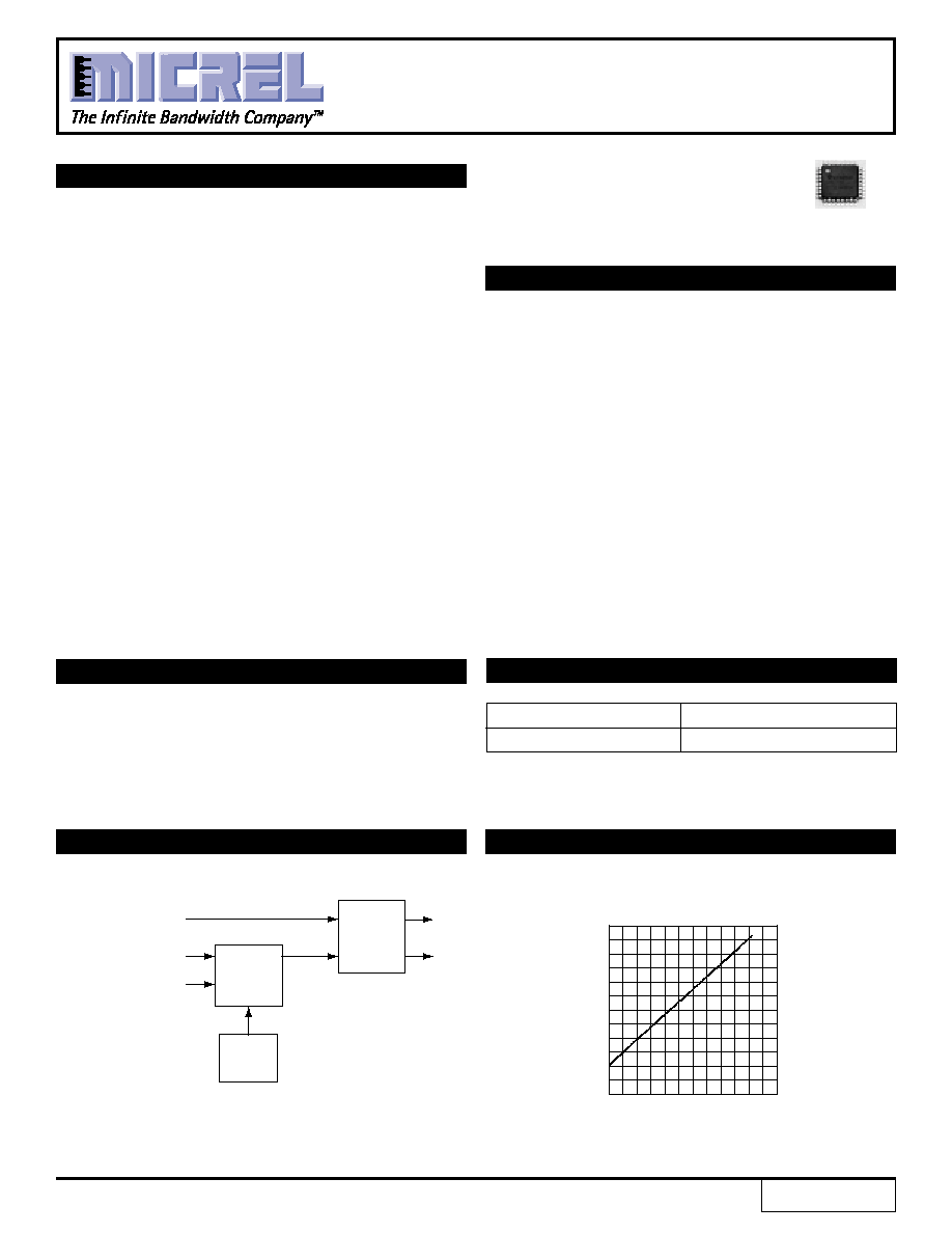
The SY100EP195V is a programmable delay line, varying
the time a logic signal takes to traverse from IN to Q. This
delay can vary from about 2.2ns to about 12.2ns. The input
can be PECL, LVPECL, NECL, or LVNECL.
The delay varies in discrete steps based on a control
word presented to SY100EP195V. The 10-bit width of this
latched control register allows for delay increments of
approximately 10ps.
An eleventh control bit allows the cascading of multiple
SY100EP195V devices, for a wider delay range. Each
additional SY100EP195V effectively doubles the delay range
available.
For maximum flexibility, the control register interface
accepts CMOS or TTL level signals, as well as the input
level at the IN
±
pins.
TYPICAL APPLICATIONS CIRCUIT
TYPICAL PERFORMANCE
IN
CONTROL
LOGIC
Data Signal
of Unknown Phase
CLOCK+
CLOCK≠
/IN
Q
/Q
D
CK
Q+
Q≠
D[9:0]
SY100EP195V
Flip-Flop
0
2000
4000
6000
8000
10000
12000
0
200 400 600 800 1000 1200
DELAY (ps)
TAP (DIGITAL WORD)
Delay vs. Tap
ECL Pro is a trademark of Micrel, Inc.
ECL ProTM
2
ECL ProTM
SY100EP195V
Micrel
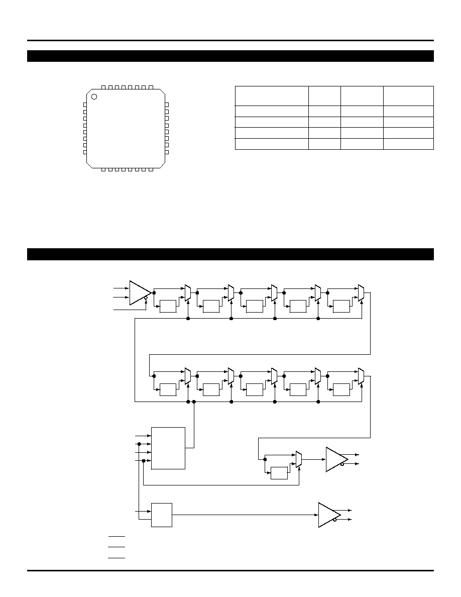
PACKAGE/ORDERING INFORMATION
Ordering Information
Package
Operating
Package
Part Number
Type
Range
Marking
SY100EP195VTI
T32-1
Commercial
SY100EP195V
SY100EP195VTCTR
(1)
T32-1
Commercial
SY100EP195V
SY100EP195VTI
(2)
T32-1
Industrial
SY100EP195V
SY100EP195VTITR
(1,2)
T32-1
Industrial
SY100EP195V
Note 1.
Tape and Reel.
Note 2.
Recommended for new designs.
VEE
D4
D5
D6
D7
D3
D2
D1
VCC
SETMAX
SETMIN
LEN
VEE
/CASCADE
CASCADE
/EN
VEE
D0
VCC
Q
/Q
VCC
VCC
NC
D8
D9
D10
IN
/IN
VBB
VEF
VCF
32 31 30 29 28 27 26 25
9 10 11 12 13 14 15 16
1
2
3
4
5
6
7
8
24
23
22
21
20
19
18
17
32-Pin TQFP (T32-1)
FUNCTIONAL BLOCK DIAGRAM
512
GD
0
1
256
GD
0
1
128
GD
0
1
64
GD
0
1
32
GD
0
1
16
GD
D[9:0]
LEN
IN
/IN
/EN
SETMIN
SETMAX
D[10]
0
1
8
GD
0
1
4
GD
0
1
2
GD
0
1
1
GD
0
1
1
GD
Q
/Q
0
1
CASCADE
/CASCADE
10-bit
Latch
Latch
V
BB
V
CF
V
EF
3
ECL ProTM
SY100EP195V
Micrel
PIN DESCRIPTION
Pin Number
Pin Name
Pin Function
23, 25, 26, 27, 29,
D[0:9]
CMOS, ECL, or TTL Select Inputs: These digital control signals adjust the amount of
30, 31, 32, 1, 2
delay from IN to Q. Please refer to the delay selection Table 1 for delay values. Figure 9
shows how to interface these inputs to various logic family standards. These inputs default
to logic low when left unconnected. Bit 0 is the least significant bit, and bit 9 is the most
significant bit.
3
D[10]
CMOS, ECL, or TTL Select Input: This input latches just like D[0:9] does. It drives the
CASCADE, /CASCADE differential pair. Use only when cascading two or more
SY100EP195V to extend the range of delays required.
4, 5
IN, /IN
ECL Input: This is the signal to be delayed. If this input pair is left unconnected, this is
equivalent to a logic low input.
6
VBB
Voltage Output: When using a single-ended logic source for IN and /IN, connect the
unused input of the differential pair to this pin. This pin can also re-bias AC coupled inputs
to IN and /IN. When used, de-couple this pin to V
CC
through an 0.01
µ
F capacitor. Limit
current sinking or sourcing to 0.5mA or less.
7
VEF
Voltage Output: Connect this pin to VCF when the D inputs are ECL. Refer to the digital
control logic standard section of the Functional Description to interface the D inputs to
CMOS or TTL.
8
VCF
Voltage Input: The voltage at this pin sets the logic transition threshold for the D inputs.
9, 24, 28
VEE
Most negative supply. Supply ground for PECL systems.
10
LEN
ECL Control Input: When logic low, the D inputs flow through. Any changes to the D inputs
reflect in the delay between IN, /IN and Q, /Q. When logic high, the logic values at D are
latched, and these latched bits determine the delay.
11
SETMIN
ECL Control Input: When logic high, the contents of the D register are reset. This sets the
delay to the minimum possible, equivalent to D[0:9] being set to 0000000000. When logic
low, the value of the D register, or the logic value of SETMAX determines the delay from
IN, /IN to Q, /Q. This input defaults to logic low when left unconnected.
12
SETMAX
ECL Control Input: When logic high and SETMIN is logic low, the contents of the D
register are set high, and the delay is set to one step greater than the maximum possible
with D[0:9] set to 1111111111. When logic low, the value of the D register, or the logic
value of SETMIN determines the delay from IN, /IN to Q, /Q. This input defaults to logic
low when left unconnected.
13, 18, 19, 22
VCC
Most positive supply: Supply ground for NECL systems. Bypass to V
EE
with 0.1
µ
F and
0.01
µ
F low ESR capacitors.
14, 15
CASCADE,
ECL Outputs: These outputs are used when cascading two or more SY100EP195V to
/CASCADE
extend the delay range required.
16
/EN
ECL Control Input: When set active low, Q, /Q are a delayed version of IN, /IN. When set
inactive high, IN, /IN are gated such that Q, /Q become a differential logic low. This input
defaults to logic low when left unconnected.
20, 21
Q, /Q
ECL Outputs: This signal pair is the delayed version of IN, /IN.
17
NC
No Connect: Leave this pin unconnected.
4
ECL ProTM
SY100EP195V
Micrel
Absolute Maximum Ratings
(Note 1)
Supply Voltage (V
CC
)
PECL Mode (V
EE
=0V) ............................. ≠0.5V to +6.0V
Supply Voltage (V
EE
)
NECL Mode (V
CC
=0V) ............................ +0.5V to ≠6.0V
Any Input Voltage (V
IN
)
PECL Mode ....................................... ≠0.5V to V
CC
+0.5V
NECL Mode ....................................... +0.5V to V
EE
≠0.5V
ECL Output Current (I
OUT
)
Continuous ............................................................. 50mA
Surge .................................................................... 100mA
I
BB
Sink/Source Current ..........................................
±
0.5mA
Lead Temperature (soldering, 10 sec.) ................... +300
∞
C
Storage Temperature (T
S
) ....................... ≠65
∞
C to +150
∞
C
ESD Rating, Note 3 ................................................. >1.5kV
Operating Ratings
(Note 2)
Supply Voltage (V
CC
)
PECL Mode (V
EE
=0V) ............................. +3.0V to +5.5V
Supply Voltage (V
EE
)
NECL Mode (V
CC
=0V) ............................ ≠3.0V to ≠5.5V
Ambient Temperature (T
A
) ......................... ≠40
∞
C to +85
∞
C
Package Thermal Resistance
TQFP-32 (
JA
)
Still-air ............................................................. 50
∞
C/W
500lfpm ............................................................ 42
∞
C/W
TQFP-32 (
JC
) ..................................................... 20
∞
C/W
T
A
= ≠40
∞
C to +85
∞
C
Symbol
Parameter
Condition
Min
Typ
Max
Units
V
CC
Power Supply Voltage (PECL)
3.0
3.3
3.6
V
4.5
5.0
5.5
V
V
EE
Power Supply Voltage (NECL)
≠3.6
≠3.3
≠3.0
V
≠5.5
≠5.0
≠4.5
V
I
EE
Power Supply Current, Note 1
No Load, Over Supply Voltage
150
180
mA
Note 1.
Required 500lfpm air flow when using +5V or ≠5V power supply.
DC ELECTRICAL CHARACTERISTICS
Note 1.
Permanent device damage may occur if ABSOLUTE MAXIMUM RATINGS are exceeded. This is a stress rating only and functional operation is
not implied at conditions other than those detailed in the operational sections of this data sheet. Exposure to ABSOLUTE MAXIMUM RATlNG
conditions for extended periods may affect device reliability.
Note 2.
The data sheet limits are not guaranteed if the device is operated beyond the operating ratings.
Note 3.
Devices are ESD sensitive. Handling precautions recommended.
5
ECL ProTM
SY100EP195V
Micrel
V
CC
= 3.3V, V
EE
= 0V; T
A
= ≠40
∞
C to +85
∞
C, Note 1, 2
Symbol
Parameter
Condition
Min
Typ
Max
Units
V
OH
Output HIGH Voltage
Figures 2, 3, 6
2155
2280
2405
mV
V
OL
Output LOW Voltage
Figures 2, 3, 6
1355
1480
1605
mV
V
IH
Input HIGH Voltage
Figures 1, 4
PECL
2075
2420
mV
CMOS
1815
mV
TTL
2000
mV
V
IL
Input LOW Voltage
Figures 1, 4
PECL
1355
1675
mV
CMOS
1485
mV
TTL
800
mV
V
BB
Output Voltage Reference
1775
1875
1975
mV
V
CF
Input Select Voltage
1610
1720
1825
mV
V
EF
Mode Connection
1900
2000
2100
mV
V
IHCMR
Input HIGH Voltage Common
Figure 5
2.0
3.3
V
Mode Range, Note 3
I
IH
Input HIGH Current
150
µ
A
I
IL
Input LOW Current
IN
0.5
µ
A
/IN
≠150
µ
A
Note 1.
Device is guaranteed to meet the DC specifications, shown in the table above, after thermal equilibrium has been established. The device is
tested in a socket such that transverse airflow of
500lfpm is maintained.
Note 2.
Input and output parameters vary 1:1 with V
CC
. V
EE
can vary +0.3V to ≠2.2V.
Note 3.
V
IHCMR
maximum varies 1:1 with V
CC
. The V
IHCMR
range is referenced to the most positive side of the differential input signal.
(100KEP) LVPECL DC ELECTRICAL CHARACTERISTICS