1
DESCRIPTION
FEATURES
3.3V/5V PECL/ECL 3GHz
DUAL DIFFERENTIAL
2:1 MULTIPLEXER
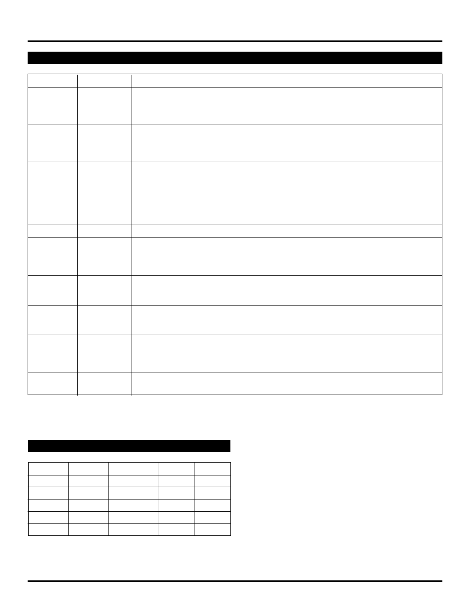
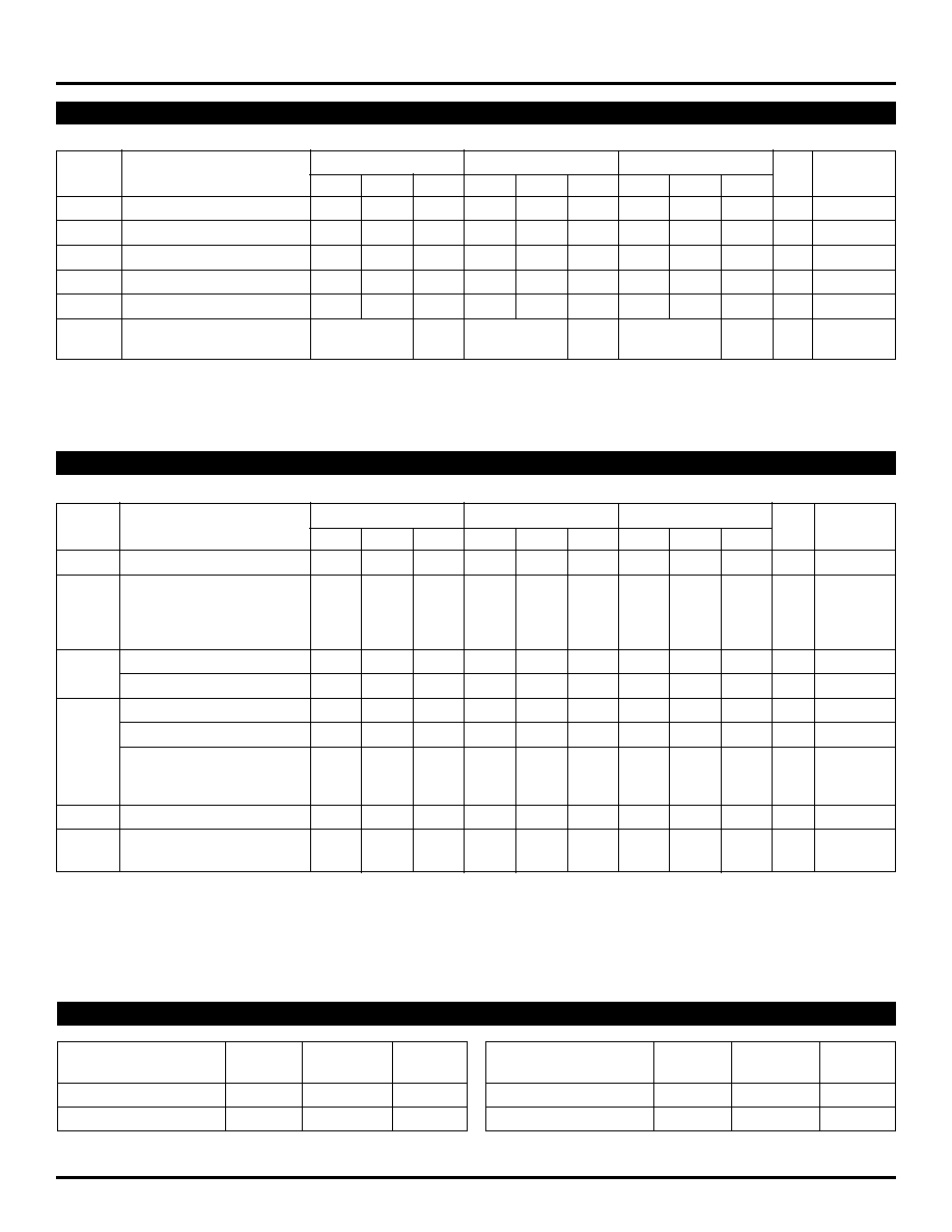
PIN CONFIGURATION/BLOCK DIAGRAM
VBB0
D0b
/D0b
D1a
/D1a
VBB1
D1b
/D1b
18 /Q0
SEL0
COM_SEL
SEL1
VEE
17
16
15
14
13
12
11
19
20
1
2
3
4
5
6
7
8
9
10
D0a
/D0a
/Q1
Q1
VCC
Q0
VCC
1
0
1
0
20-pin TSSOP Package
ECL ProTM
SY100EP56V
FINAL
s
Dual, fully differential 2:1 PECL/ECL multiplexer
s
Guaranteed AC parameters over temperature/
voltage:
∑ > 3GHz f
MAX
(toggle)
∑ < 100ps within device skew
∑ < 230ps rise/fall times
∑ < 500ps propagation delay
s
Flexible power supply: 3.0V to 5.5V
s
Wide operating temperature range: ≠40
∞
C to +85
∞
C
s
V
BB
reference for AC-coupled and single-ended
applications
s
Both channels have independent input select or
common select control
s
100k PECL/ECL compatible logic
s
Available in 20-pin TSSOP package
The SY100EP56V is a high-speed, low-skew, fully
differential Dual PECL/ECL 2:1 multiplexer. This device is a
pin-for-pin, plug-in replacement to the MC10/100EP56DT.
Two separate 2:1 multiplexers (Channel 0 and Channel 1)
with dedicated select control pins (SEL0 and SEL1) are
implemented in a 20-pin TSSOP package. The signal-path
inputs (D0a, D0b and D1a, D1b) accept differential signals
as low as 150mV pk-pk. For applications that require
common select control for both channels A & B, a common
select pin (COM_SEL) is available. All I/O pins are 100k
PECL/ECL logic compatible.
AC≠performance is guaranteed over the industrial ≠40
∞
C
to +85
∞
C temperature range and 3.0V to 5.5V supply voltage
range. This device will operate in PECL/LVPECL or ECL/
LVECL mode. The 500ps max (400 typ) propagation delay
is matched for all signal and logic select paths: D-to-Q
OUT
,
SEL-to-Q
OUT
, and COM_SEL-to-Q
OUT
. Two V
BB
output
reference pins (approx equal to V
CC
≠1.4V) are available
for AC≠coupled or single-ended applications.
The SY100EP56V is part of Micrel's high-speed, Precision
Edge timing and distribution family. For applications that
require a different I/O combination, consult the Micrel website
at
www.micrel.com
, and choose from a comprehensive
product line of high-speed, low skew fanout buffers,
translators, and clock dividers.
Rev.: C
Amendment: /0
Issue Date:
March 2003
Micrel Semiconductor
ON Semiconductor
SY100EP56VK4I
MC100EP56DT
SY100EP56VK4ITR
MC100EP56DTR2
CROSS REFERENCE TABLE
ECL ProTM
ECL Pro is a trademark of Micrel, Inc.
2
ECL ProTM
SY100EP56V
Micrel
PIN DESCRIPTION
Pin
Pin Number
Function
D0a, /D0a
1, 2,
Channel 0 PECL/ECL differential signal inputs. Multiplexing of these two differential inputs is
D0b, /D0b
4, 5
controlled by SEL0, or COM_SEL. The signal inputs include internal 75k
pull-down resistors.
Default condition is LOW when left floating. The input signal should be terminated externally.
See "
Termination
" section
D1a, /D1a
6, 7
Channel 1 PECL/ECL differential signal inputs. Multiplexing of these two differential inputs is
D1b, /D1b
9, 10
controlled by SEL1, or COM_SEL. The signal inputs include internal 75k
pull-down resistors.
Default condition is a logic LOW when left floating. The input signal should be terminated
externally. See "
Termination
" section
VBB0, VBB1
3, 8
Channel 0 and Channel 1 reference output voltage. This reference is typically used to bias the
unused inverting input for single-ended input applications, or as the termination point for AC≠
coupled differential input applications. V
BB
reference value is approximately V
CC
≠1.4V, and tracks
V
CC
1:1. Maximum sink/source capability is 0.50mA. For single ended PECL inputs, connect to
the unused input through a 50
resistor. Decouple the V
BB
pin with a 0.01
µ
F capacitor. For PECL/
LVPECL inputs, the decoupling capacitor is connected to V
CC
, since PECL signals are referenced
to V
CC
. Leave floating if not used.
VEE
11
Negative Power Supply: For PECL/LVPECL applications, connect to GND.
/Q1, Q1
12, 13
Channel 1 100KEP PECL/ECL compatible differential output. PECL/ECL termination is with a 50
resistor to V
CC
≠2V. Unused output pairs may be left floating. Unused single-ended outputs must
have a balanced load. For AC-coupled applications, the output stage emitter follower must have a
DC current path to ground. See "
Termination
" section.
SEL1, SEL0
15, 17
100KEP PECL/ECL compatible Channel 1 and Channel 0 MUX select control. See "
MUX Select
Truth Table
." Each pin includes an internal 75k
pull-down resistor. Default condition when left
floating is LOW.
COM_SEL
16
100KEP PECL/ECL compatible Channel 1 and Channel 0 Common MUX select control. This is
the common select control pin for both Channels 0 and 1. Includes an internal 75k
pull-down
resistor. Default condition when left floating is LOW. Leave floating when not used.
/Q0, Q0
18, 19
Channel 0 100K EP PECL/ECL compatible differential output. PECL/ECL termination is with a
50
resistor to V
CC
≠2V. Unused output pairs may be left floating. Unused single-ended outputs
must have a balanced load. For AC≠coupled applications, the output stage emitter follower must
have a DC current path to ground. See "
Termination
" section.
VCC
14, 20
Positive Power Supply: Both V
CC
pins must be connected to the same power supply externally.
Bypass with 0.1
µ
F//0.01
µ
F low ESR capacitors.
MUX SELECT TRUTH TABLE
SEL0
SEL1
COM_SEL
Q0, /Q0
Q1, /Q1
X
X
H
a
a
L
L
L
b
b
L
H
L
b
a
H
H
L
a
a
H
L
L
a
b
3
ECL ProTM
SY100EP56V
Micrel
Symbol
Rating
Value
Unit
V
CC
-- V
EE
Power Supply Voltage
6.0
V
V
IN
Input Voltage (V
CC
= 0V, V
IN
not more negative than V
EE
)
≠6.0 to 0
V
Input Voltage (V
EE
= 0V, V
IN
not more positive than V
CC
)
+6.0 to 0
V
I
OUT
Output Current
≠Continuous
50
mA
≠Surge
100
I
BB
V
BB
Sink/Source Current
(2)
±
0.5
mA
T
A
Operating Temperature Range
≠40 to +85
∞
C
T
store
Storage Temperature Range
≠65 to +150
∞
C
JA
Package Thermal Resistance
≠Still-Air (single-layer PCB)
115
∞
C/W
(Junction-to-Ambient)
≠Still-Air (multi-layer PCB)
75
≠500lfpm (multi-layer PCB)
65
JC
Package Thermal Resistance
21
∞
C/W
(Junction-to-Case)
Note 1.
Permanent device damage may occur if ABSOLUTE MAXIMUM RATINGS are exceeded. This is a stress rating only and functional operation
is not implied at conditions other than those detailed in the operational sections of this data sheet. Exposure to ABSOLUTE MAXIMUM
RATlNG conditions for extended periods may affect device reliability.
Note 2.
Due to the limited drive capability, the V
BB
reference should only be used for inputs from the same package device (i.e., do not use for other
devices).
ABSOLUTE MAXIMUM RATINGS
(1)
T
A
= ≠40
∞
C
T
A
= +25
∞
C
T
A
= +85
∞
C
Symbol
Parameter
Min.
Typ.
Max.
Min.
Typ.
Max.
Min.
Typ.
Max.
Unit
Condition
V
CC
Power Supply Voltage
V
(PECL)
4.5
5.0
5.5
4.5
5.0
5.5
4.5
5.0
5.5
(LVPECL)
3.0
3.3
3.8
3.0
3.3
3.8
3.0
3.3
3.8
(ECL)
≠5.5
≠5.0
≠4.5
≠5.5
≠5.0
≠4.5
≠5.5
≠5.0
≠4.5
(LVECL)
≠3.8
≠3.3
≠3.0
≠3.8
≠3.3
≠3.0
≠3.8
≠3.3
≠3.0
I
EE
Supply Current
--
50
65
--
50
65
--
50
65
mA
No Load
I
IH
Input HIGH Current
--
--
150
--
--
150
--
--
150
µ
A
V
IN
= V
IH
I
IL
Input LOW Current
All Inputs
0.5
--
--
0.5
--
--
0.5
--
--
µ
A
V
IN
= V
IL
C
IN
Input Capacitance (TSSOP)
--
--
--
--
1.0
--
--
--
--
pF
Note 1.
100KEP circuits are designed to meet the DC specifications shown in the above table after thermal equilibrium has been established. The
circuit is in a test socket or mounted on a printed circuit board and traverse airflow greater than 500lfpm is maintained.
DC ELECTRICAL CHARACTERISTICS
(1)
4
ECL ProTM
SY100EP56V
Micrel
T
A
= ≠40
∞
C
T
A
= +25
∞
C
T
A
= +85
∞
C
Symbol
Parameter
Min.
Typ.
Max.
Min.
Typ.
Max.
Min.
Typ.
Max.
Unit
Condition
V
IL
Input LOW Voltage
1355
--
1675
1355
--
1675
1355
--
1675
mV
(Single-Ended)
V
IH
Input HIGH Voltage
2075
--
2420
2075
--
2420
2075
--
2420
mV
(Single-Ended)
V
OL
Outuput LOW Voltage
1355
1480
1605
1355
1480
1605
1355
1480
1605
mV
50
to V
CC
≠2V
V
OH
Output HIGH Voltage
2155
2280
2405
2155
2280
2405
2155
2280
2405
mV
50
to V
CC
≠2V
V
BB
Output Reference Voltage
1775
1875
1975
1775
1875
1975
1775
1875
1975
mV
V
IHCMR
Input HIGH Voltage
(2)
2.0
--
V
CC
2.0
--
V
CC
2.0
--
V
CC
V
Common Mode Range
(100KEP) LVPECL DC ELECTRICAL CHARACTERISTICS
(1)
V
CC
= 3.3V
±
10%, V
EE
= 0V
Note 1.
100KEP circuits are designed to meet the DC specifications shown in the above table after thermal equilibrium has been established. The
circuit is in a test socket or mounted on a printed circuit board and traverse airflow greater than 500lfpm is maintained. Input and output
parameters are at V
CC
= 3.3V. They vary 1:1 with V
CC
.
Note 2.
The V
IHCMR
range is referenced to the most positive side of the differential input signal.
T
A
= ≠40
∞
C
T
A
= +25
∞
C
T
A
= +85
∞
C
Symbol
Parameter
Min.
Typ.
Max.
Min.
Typ.
Max.
Min.
Typ.
Max.
Unit
Condition
V
IL
Input LOW Voltage
3055
--
3375
3055
--
3375
3055
--
3375
mV
(Single-Ended)
V
IH
Input HIGH Voltage
3775
--
4120
3775
--
4120
3775
--
4120
mV
(Single-Ended)
V
OL
Outuput LOW Voltage
3055
3180
3305
3055
3180
3305
3055
3180
3305
mV
50
to V
CC
≠2V
V
OH
Output HIGH Voltage
3855
3980
4105
3855
3980
4105
3855
3980
4105
mV
50
to V
CC
≠2V
V
BB
Output Reference Voltage
3475
3575
3675
3475
3575
3675
3475
3575
3675
mV
V
IHCMR
Input HIGH Voltage
(2)
2.0
--
V
CC
2.0
--
V
CC
2.0
--
V
CC
V
Common Mode Range
(100KEP) PECL DC ELECTRICAL CHARACTERISTICS
(1)
V
CC
= 5.0V
±
10%, V
EE
= 0V
Note 1.
100KEP circuits are designed to meet the DC specifications shown in the above table after thermal equilibrium has been established. The
circuit is in a test socket or mounted on a printed circuit board and traverse airflow greater than 500lfpm is maintained. Input and output
parameters are at V
CC
= 5.0V. They vary 1:1 with V
CC
.
Note 2.
The V
IHCMR
range is referenced to the most positive side of the differential input signal.
5
ECL ProTM
SY100EP56V
Micrel
T
A
= ≠40
∞
C
T
A
= +25
∞
C
T
A
= +85
∞
C
Symbol
Parameter
Min.
Typ.
Max.
Min.
Typ.
Max.
Min.
Typ.
Max.
Unit
Condition
V
IL
Input LOW Voltage
≠1945
--
≠1625 ≠1945
--
≠1625 ≠1945
--
≠1625
mV
V
IH
Input HIGH Voltage
≠1225
--
≠880
≠1225
--
≠880
≠1225
--
≠880
mV
V
OL
Outuput LOW Voltage
≠1945 ≠1820 ≠1695 ≠1945 ≠1820 ≠1695 ≠1945 ≠1820 ≠1695
mV
50
to V
CC
≠2V
V
OH
Output HIGH Voltage
≠1145 ≠1020
≠895
≠1145 ≠1020
≠895
≠1145 ≠1020
≠895
mV
50
to V
CC
≠2V
V
BB
Output Reference Voltage
≠1525 ≠1425 ≠1325 ≠1525 ≠1425 ≠1325 ≠1525 ≠1425 ≠1325
mV
V
IHCMR
Input HIGH Voltage
(2)
V
EE
+2.0
0.0
V
EE
+2.0
0.0
V
EE
+2.0
0.0
V
Common Mode Range
(100KEP) ECL/LVECL DC ELECTRICAL CHARACTERISTICS
(1)
V
CC
= 0V, V
EE
= ≠5.5V to ≠3.0V
Note 1.
100KEP circuits are designed to meet the DC specifications shown in the above table after thermal equilibrium has been established. The
circuit is in a test socket or mounted on a printed circuit board and traverse airflow greater than 500lfpm is maintained.
Note 2.
The V
IHCMR
range is referenced to the most positive side of the differential input signal.
T
A
= ≠40
∞
C
T
A
= +25
∞
C
T
A
= +85
∞
C
Symbol
Parameter
Min.
Typ.
Max.
Min.
Typ.
Max.
Min.
Typ.
Max.
Unit
Condition
f
MAX
Max. Toggle Frequency
(1)
3
--
--
3
--
--
3
--
--
GHz
t
PLH
Propagation Delay (Differential)
t
PHL
D to Q, /Q
230
290
450
230
290
470
230
300
500
ps
SEL to Q, /Q
250
300
450
250
320
470
250
330
500
ps
COM_SEL to Q, /Q
250
350
450
250
360
470
250
400
500
ps
t
SKEW
Within-Device Skew
(2)
Q, /Q
--
50
100
--
50
100
--
50
100
ps
Part-to-Part Skew
(2)
--
--
200
--
--
200
--
--
200
ps
t
JITTER
Cycle-to-Cycle Jitter (rms)
--
0.2
< 1
--
0.2
< 1
--
0.2
< 1
ps
rms
Random Jitter
--
--
--
--
<1
--
--
--
--
ps
rms
Note 3
Deterministic Jitter
@1.25Gbps
--
--
--
--
<25
--
--
--
--
ps
pk-pk
Note 4
@2.5Gbps
--
--
--
--
<50
--
--
--
--
V
DIFF
Input Voltage (Differential)
150
800
1200
150
800
1200
150
800
1200
mV
t
r,
t
f
Output Rise/Fall Time Q, /Q
--
120
170
--
130
180
--
150
230
ps
(20% to 80%)
AC ELECTRICAL CHARACTERISTICS
V
CC
= 0V; V
EE
= ≠3.0V to ≠5.5V or V
CC
= 3.0V to 5.5V, V
EE
= 0V
Note 1.
Measured with 750mV input signal, 50% duty cycle. Output swing
400mV. All loading with a 50
to V
CC
≠2.0V.
Note 2.
Skew is measured between outputs under identical transitions. Duty cycle skew is defined only for differential operation when the delays are
measured from the cross point of the inputs to the cross point of the outputs.
Note 3.
RJ is measured with a K28.7 comma detect character pattern, measured at 1.25Gbps and 2.5Gbps.
Note 4.
DJ is measured at 1.25Gbps and 2.5Gbps, with both K28.5 and 2
23
≠1 PRBS pattern.
Ordering
Package
Operating
Package
Code
Type
Range
Marking
SY100EP56VK4C
K4-20-1
Commercial
XEP56V
SY100EP56VK4CTR
(1)
K4-20-1
Commercial
XEP56V
Note 1.
Tape and Reel.
Note 2.
Recommended for new designs.
PRODUCT ORDERING CODE
Ordering
Package
Operating
Package
Code
Type
Range
Marking
SY100EP56VK4I
(2)
K4-20-1
Industrial
XEP56V
SY100EP56VK4ITR
(1, 2)
K4-20-1
Industrial
XEP56V