Pin
Function
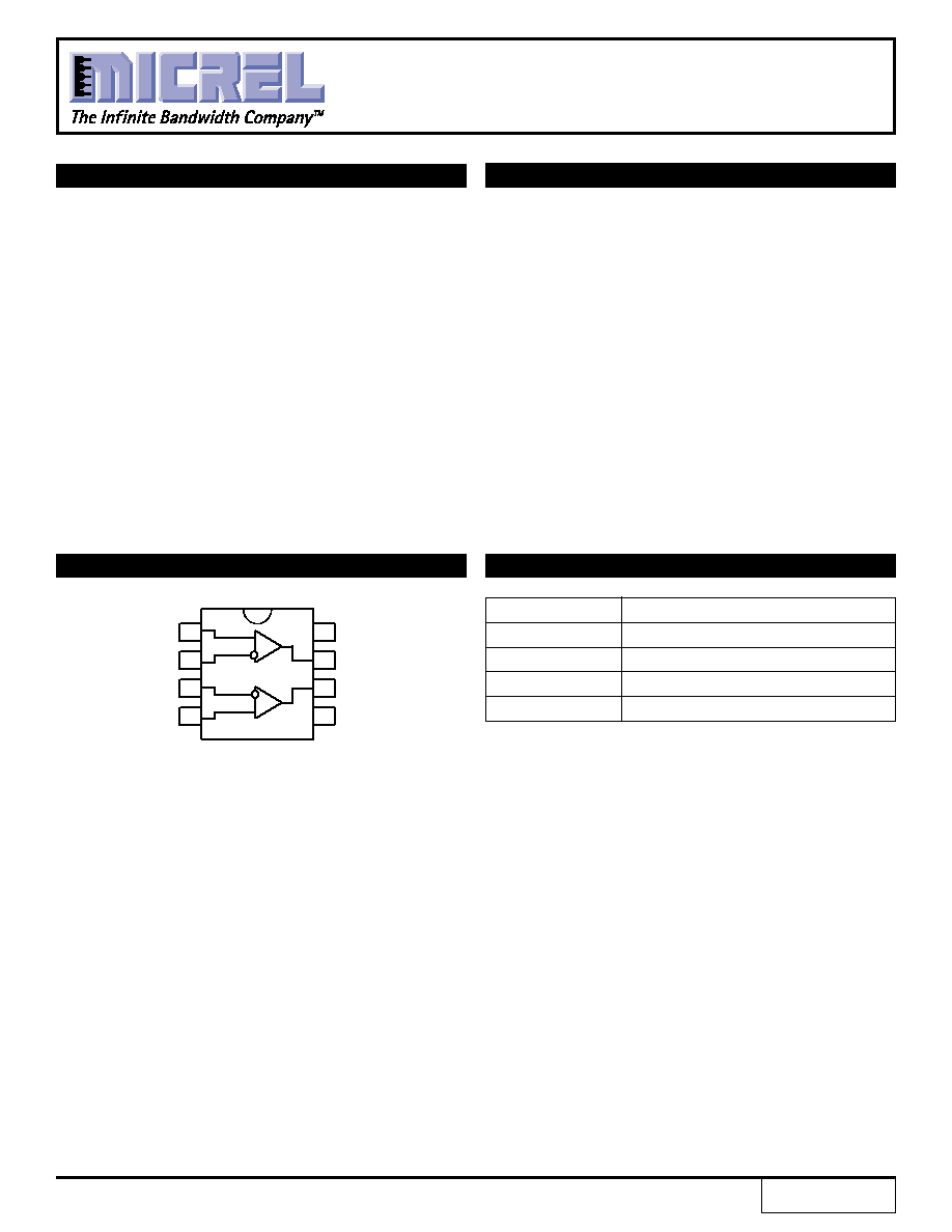
Q0, Q1
LVTTL Outputs
D0, /D0, D1, /D1
Differential LVPECL Inputs
V
CC
Positive Supply
GND
Ground
DESCRIPTION
s
3.3V power supply
s
1.9ns typical propagation delay
s
Maximum frequency > 275MHz
s
Differential LVPECL inputs
s
24mA LVTTL outputs
s
Flow-through pinouts
s
Internal input resistors: pulldown on D, pulldown
and pullup on /D
s
Q output will default LOW with inputs open or at
Ground
s
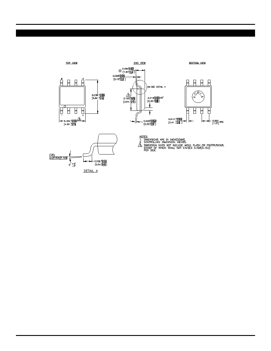
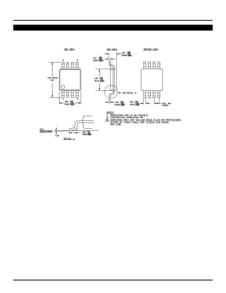
Available in 8-pin MSOP and SOIC packages
The SY100EPT23L is a dual differential LVPECL-to-
LVTTL translator. Because LVPECL (Low Voltage Positive
ECL) levels are used, only +3.3V and ground are required.
The tiny 8-pin MSOP and dual-gate design of the EPT23L
makes it ideal for applications which require the
translation of a clock and data signal.
The EPT23L is available in only the ECL 100K
standard. Since there are no LVPECL outputs or an
external V
BB
reference, the EPT23L does not require
both ECL standard versions. The inputs can accept 10K
voltage levels and any standard differential LVPECL input
referenced from a V
CC
of +3.3V
FEATURES
3.3V DUAL DIFFERENTIAL
LVPECL-to-LVTTL
TRANSLATOR
PIN NAMES
PIN CONFIGURATION/BLOCK DIAGRAM
1
D0
/D0
/D1
D1
8
V
CC
Q0
GND
7
6
5
2
3
4
Q1
LVPECL
LVTTL
(Available in 8-pin SOIC and 8-pin MSOP)
SY100EPT23L
1
Rev.: A
Amendment: 1
Issue Date:
July 2000
2
SY100EPT23L
Micrel
TRUTH TABLE
D
/D
Q
L
H
L
H
L
H
Open
Open
L
Symbol
Paramter
Value
Unit
V
CC
Power Supply Voltage
≠0.5 to +3.8
V
V
I
PECL Input Voltage
0V to V
CC
+0.5
V
V
O
Voltage Applied to
≠0.5 to V
CC
V
Output at HIGH State
I
O
Current Applied to
Twice the
mA
Output at LOW State
Rated I
OL
T
store
Storage Temperature
≠65 to +150
∞
C
T
A
Operating Temperature
≠40 to +85
∞
C
NOTE:
1. Permanent device damage may occur if ABSOLUTE MAXIMUM RATINGS
are exceeded. This is a stress rating only and functional operation is not
implied at conditions other than those detailed in the operational sections
of this data sheet. Exposure to ABSOLUTE MAXIMUM RATlNG conditions
for extended periods may affect device reliability.
ABSOLUTE MAXIMUM RATINGS
(1)
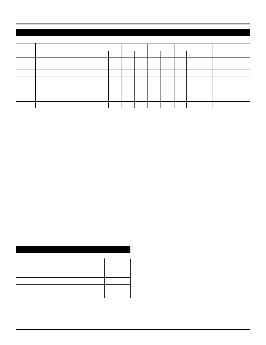
LVTTL DC ELECTRICAL CHARACTERISTICS
T
A
= ≠40
∞
C
T
A
= 0
∞
C
T
A
= +25
∞
C
T
A
= +85
∞
C
Symbol
Parameter
Min.
Max.
Min.
Max.
Min.
Max.
Min.
Max.
Unit
Condition
V
OH
Output HIGH Voltage
2.0
--
2.0
--
2.0
--
2.0
--
V
I
OH
= ≠3.0mA
V
OL
Output LOW Voltage
--
0.5
--
0.5
--
0.5
--
0.5
V
I
OL
= 24mA
I
CC
Power Supply Current
--
30
--
30
--
30
--
30
mA
I
OS
Output Short Circuit Current
≠80
≠240
≠80
≠240
≠80
≠240
≠80
≠240
mA
V
OUT
= 0V
V
CC
= +3.3V
±
5%
T
A
= ≠40
∞
C
T
A
= 0
∞
C
T
A
= +25
∞
C
T
A
= +85
∞
C
Symbol
Parameter
Min.
Typ.
Max.
Min.
Typ.
Max.
Min.
Typ.
Max.
Min.
Typ.
Max.
Unit
I
IH
Input HIGH Current
--
--
150
--
--
150
--
--
150
--
--
150
µ
A
I
IL
Input LOW Current
0.5
--
--
0.5
--
--
0.5
--
--
0.5
--
--
µ
A
V
CMR
Common Mode Range
1.5
--
V
CC
1.5
--
V
CC
1.5
--
V
CC
1.5
--
V
CC
V
V
PP
Minimum Peak-to-Peak
Input
(1)
200
--
--
200
--
--
200
--
--
200
--
--
mV
V
IH
Input HIGH Voltage
(2)
2070
--
2420
2130
--
2460
2135
--
2490
2130
--
2565
mV
V
IL
Input LOW Voltage
(2)
1350
--
1825
1350
--
1825
1350
--
1825
1350
--
1825
mV
V
CC
= +3.3V
±
5%
NOTES:
1. 200mV input guarantees full logic at output.
2. These values are for V
CC
= 3.3V. Level Specifications will vary 1:1 with V
CC
.
LVPECL DC ELECTRICAL CHARACTERISTICS
3
SY100EPT23L
Micrel
PRODUCT ORDERING CODE
Ordering
Package
Operating
V
CC
Range
Code
Type
Range
(V)
SY100EPT23LZC
Z8-1
Commercial
+3.3
±
5%
SY100EPT23LZCTR
Z8-1
Commercial
+3.3
±
5%
SY100EPT23LKC
K8-1
Commercial
+3.3
±
5%
SY100EPT23LKCTR
K8-1
Commercial
+3.3
±
5%
T
A
= ≠40
∞
C
T
A
= 0
∞
C
T
A
= +25
∞
C
T
A
= +85
∞
C
Symbol
Parameter
Min.
Max.
Min.
Max.
Min.
Max.
Min.
Max.
Unit
Condition
t
PLH
Propagation Delay
1.5
2.5
1.5
2.5
1.5
2.5
1.5
2.5
ns
C
L
= 20pF
t
PHL
t
skpp
Part-to-Part Skew
(1,4)
--
0.5
--
0.5
--
0.5
--
0.5
ns
C
L
= 20pF
t
skew++
Within-Device Skew
(2,4)
--
0.3
--
0.3
--
0.3
--
0.3
ns
C
L
= 20pF
t
skew≠ ≠
Within-Device Skew
(3,4)
--
0.3
--
0.3
--
0.3
--
0.3
ns
C
L
= 20pF
t
r
Output Rise/Fall Time
0.5
1.0
0.5
1.0
0.5
1.0
0.5
1.0
ns
C
L
= 20pF
t
f
1.0V to 2.0V
f
MAX
Maximum Input Frequency
(5,6)
275
--
275
--
275
--
275
--
MHz
C
L
= 20pF
AC ELECTRICAL CHARACTERISTICS
V
CC
= +3.3V
±
5%
NOTES:
1. Device-to-Device Skew considering HIGH-to-HIGH transitions at common V
CC
level.
2. Within-Device Skew considering HIGH-to-HIGH transitions at common V
CC
level.
3. Within-Device Skew considering LOW-to-LOW transitions at common V
CC
level.
4. All skew parameters are guaranteed but not tested.
5. Frequency at which guaranteed for functionality. V
OH
and V
OL
levels are guaranteed at DC only.
6. The f
MAX
value is specified as the minimum guaranteed maximum frequency. Actual operational maximum frequency may be greater.