
DESCRIPTION
FEATURES
ClockWorksTM
SY10H641L
SY100H641L
FINAL
s
3.3V power supply
s
PECL-to-TTL version of popular ECLinPS E111
s
Guaranteed low skew specification
s
Latched input
s
Differential ECL internal design
s
V
BB
output for single-ended operation
s
Reset/enable
s
Extra TTL and ECL power/ground pins
s
Choice of ECL compatibility: MECL 10KH (10Hxxx)
or 100K (100Hxxx)
s
Available in 28-pin PLCC package
The SY10/100H641L are single supply, low skew
translating 1:9 clock drivers. Devices in the Micrel-
Synergy H600 translator series utilize the 28-lead PLCC
for optimal power pinning, signal flow-through and
electrical performance.
The devices feature a 24mA TTL output stage with
AC performance specified into a 20pF load capacitance.
A latch is provided on-chip. When LEN is LOW (or left
open, in which case it is pulled LOW by the internal pull-
downs), the latch is transparent. A HIGH on the enable
pin (/EN) forces all outputs LOW.
The 10H version is compatible with MECL 10KH ECL
logic levels. The 100H version is compatible with 100K
levels.
3.3V SINGLE SUPPLY
1:9 PECL-TO-TTL
18
17
16
15
14
13
12
5
6
7
8
9
10 11
26
27
28
1
2
3
4
TOP VIEW
PLCC
25 24 23 22 21 20 19
V
T
Q
7
V
T
Q
8
G
T
Q
6
G
T
G
T
Q
5
V
T
Q
4
V
T
Q
3
G
T
Q
2
Q
1
V
T
Q
0
G
T
G
T
V
T
V
BB
D
V
E
LEN
G
E
D
EN
PIN CONFIGURATION
BLOCK DIAGRAM
D
Q
0
Q
1
Q
2
Q
3
V
BB
EN
D
Q
4
Q
5
Q
6
Q
7
Q
8
LEN
D
Q
PECL Input
TTL Outputs
Pin
Function
G
T
TTL Ground (0V)
V
T
TTL V
CC
(+3.0V)
V
E
ECL V
CC
(+3.0V)
G
E
ECL Ground (0V)
D, /D
Signal Input (PECL)
V
BB
V
BB
Reference Output (PECL)
Q
0
≠ Q
8
Signal Outputs (TTL)
/EN
Enable Input (PECL)
LEN
Latch Enable Input (PECL)
PIN NAMES
1
Rev.: E
Amendment: /0
Issue Date:
March 2002
2
ClockWorksTM
SY10H641L
SY100H641L
Micrel
D
LEN
/EN
Q
L
L
L
L
H
L
L
H
X
H
L
Q
0
X
X
H
L
TRUTH TABLE
Symbol
Rating
Value
Unit
V
E
(ECL)
Power Supply
≠0.5 to +7.0
V
V
T
(TTL)
Voltage
≠0.5 to +7.0
V
I
(ECL)
Input Voltage
0.0 to V
E
V
V
OUT
(TTL)
Disabled 3-State
0.0 to V
T
V
Output
I
OUT
(ECL)
Output Current
mA
- Continuous
50
- Surge
100
T
store
Storage Temperature
≠65 to +150
∞
C
T
A
Operating Temperature
0 to +85
∞
C
ABSOLUTE MAXIMUM RATINGS
(1)
NOTE:
1. Do not exceed.
DC ELECTRICAL CHARACTERISTICS
V
T
= V
E
= +3.0V to +3.6V
T
A
= 0
∞
C
T
A
= +25
∞
C
T
A
= +85
∞
C
Symbol
Parameter
Min.
Max.
Min.
Max.
Min.
Max.
Unit
Condition
I
EE
Power Supply Current
ECL
--
30
--
30
--
30
mA
V
E
Pin
I
CCH
TTL
--
30
--
30
--
30
Total all V
T
pins
I
CCL
--
35
--
35
--
35
TTL DC ELECTRICAL CHARACTERISTICS
V
T
= V
E
= +3.0V to +3.6V
T
A
= 0
∞
C
T
A
= +25
∞
C
T
A
= +85
∞
C
Symbol
Parameter
Min.
Max.
Min.
Max.
Min.
Max.
Unit
Condition
V
OH
Output HIGH Voltage
2.0
--
2.0
--
2.0
--
V
I
OH
= ≠3.0mA
V
OL
Output LOW Voltage
--
0.5
--
0.5
--
0.5
V
I
OL
= 24mA
I
OS
Output Short Circuit Current
≠100
--
≠100
--
≠100
--
mA
V
OUT
= 0V
V
T
= V
E
= +3.0V to +3.6V
T
A
= 0
∞
C
T
A
= +25
∞
C
T
A
= +85
∞
C
Symbol
Parameter
Min.
Max.
Min.
Max.
Min.
Max.
Unit
Condition
I
IH
Input HIGH Current
--
225
--
175
--
175
µ
A
--
I
IL
Input LOW Current
0.5
--
0.5
--
0.5
--
µ
A
--
V
IH
Input HIGH Voltage
(1)
2.130
2.460
2.170
2.490
2.240
2.580
V
V
E
= 3.3V
V
IL
Input LOW Voltage
(1)
1.350
1.820
1.350
1.820
1.350
1.855
V
V
E
= 3.3V
V
BB
Output Reference Voltage
(1)
1.920
2.030
1.950
2.050
1.990
2.110
V
V
E
= 3.3V
NOTE:
1. V
IH
, V
IL
and V
BB
are referenced to V
E
and will vary 1:1 with the power supply. The levels shown are for V
E
= +3.3V.
10H ECL DC ELECTRICAL CHARACTERISTICS
3
ClockWorksTM
SY10H641L
SY100H641L
Micrel
100H ECL DC ELECTRICAL CHARACTERISTICS
V
T
= V
E
= +3.0V to +3.6V
T
A
= 0
∞
C
T
A
= +25
∞
C
T
A
= +85
∞
C
Symbol
Parameter
Min.
Max.
Min.
Max.
Min.
Max.
Unit
Condition
I
IH
Input HIGH Current
--
225
--
175
--
175
µ
A
--
I
IL
Input LOW Current
0.5
--
0.5
--
0.5
--
µ
A
--
V
IH
Input HIGH Voltage
(1)
2.135
2.420
2.135
2.420
2.135
2.420
V
V
E
= 3.3V
V
IL
Input LOW Voltage
(1)
1.490
1.825
1.490
1.825
1.490
1.825
V
V
E
= 3.3V
V
BB
Output Reference Voltage
(1)
1.920
2.040
1.920
2.040
1.920
2.040
V
V
E
= 3.3V
NOTE:
1. V
IH
, V
IL
and V
BB
are referenced to V
E
and will vary 1:1 with the power supply. The levels shown are for V
E
= +3.3V.
AC ELECTRICAL CHARACTERISTICS
V
T
= V
E
= +3.0V to +3.6V
T
A
= 0
∞
C
T
A
= +25
∞
C
T
A
= +85
∞
C
Symbol
Parameter
Min.
Max.
Min.
Max.
Min.
Max.
Unit
Condition
t
PLH
Propagation Delay
2.0
3.0
2.0
3.0
2.0
3.0
ns
C
L
= 20pF
t
PHL
D to Output
2.5
3.5
2.5
3.5
2.5
3.5
t
skpp
Part-to-Part Skew
(1,4)
--
0.5
--
0.5
--
0.5
ns
C
L
= 20pF
t
skew++
Within-Device Skew
(2,3,4)
--
0.3
(7)
--
0.3
(7)
--
0.3
(7)
ns
C
L
= 20pF
t
skew≠ ≠
--
0.35
(8)
--
0.35
(8)
--
0.35
(8)
ns
C
L
= 20pF
t
PLH
Propagation Delay
2.0
3.5
2.0
3.5
2.0
3.5
ns
C
L
= 20pF
t
PHL
LEN to Output
t
PLH
Propagation Delay
2.0
3.5
2.0
3.5
2.0
3.5
ns
C
L
= 20pF
t
PHL
/EN to Output
t
r
Output Rise/Fall Time
--
1.7
--
1.7
--
1.7
ns
C
L
= 20pF
t
f
1.0V to 2.0V
--
1.6
--
1.6
--
1.6
f
MAX
Maximum Input Frequency
(5,6)
135
--
135
--
135
--
MHz
--
Pulse Width
1.5
--
1.5
--
1.5
--
ns
--
--
Recovery Time
1.25
--
1.25
--
1.25
--
ns
--
t
S
Set-up Time
0.5 (typ.)
0.5 (typ.)
0.5 (typ.)
ns
--
t
H
Hold Time
0.5 (typ.)
0.5 (typ.)
0.5 (typ.)
ns
--
NOTES:
1. Device-to-Device Skew considering HIGH-to-HIGH transitions at common V
CC
level.
2. Within-Device Skew considering HIGH-to-HIGH transitions at common V
CC
level.
3. Within-Device Skew considering LOW-to-LOW transitions at common V
CC
level.
4. All skew parameters are guaranteed but not tested.
5. Frequency at which output levels will meet a 0.8V to 2.0V minimum swing.
6. The f
MAX
value is specified as the minimum guaranteed maximum frequency. Actual operational maximum frequency may be greater.
7. V
T
= V
E
= +3.15V to +3.45V, (i.e. V
E
+/≠ 5%).
8. V
T
= V
E
= +3.0V to +3.6V, (i.e. V
E
+/≠ 10%).
4
ClockWorksTM
SY10H641L
SY100H641L
Micrel
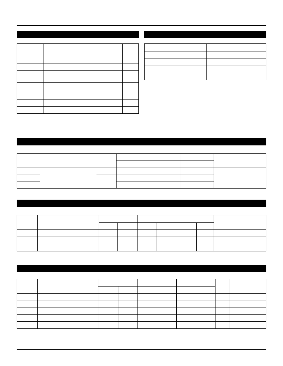
TTL SWITCHING CIRCUIT
PULSE
GENERATOR
IN
OUT
PECL
V
EE
V
CC
& V
CCO
TTL
DEVICE
UNDER
TEST
CH A
OSCILLOSCOPE
CH B
50
COAX
450
USE 0.1µF CAPACITORS
FOR DECOUPLING.
USE OSCILLOSCOPE
INTERNAL 50
LOAD
FOR TERMINATION.
50
COAX
50
COAX
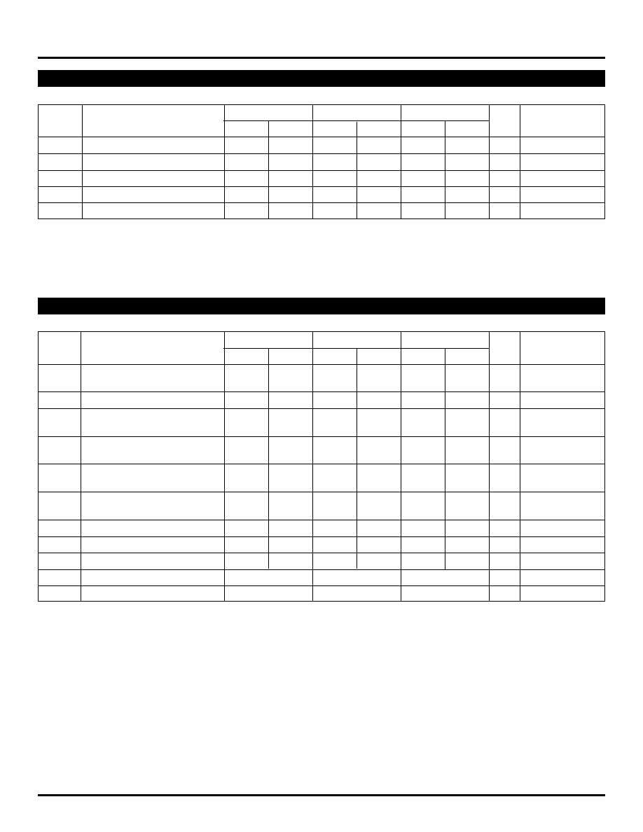
ECL/TTL PROPAGATION DELAY -- SINGLE ENDED
V
IN
V
OUT
50%
1.5V
T
pd++
T
pd≠ ≠
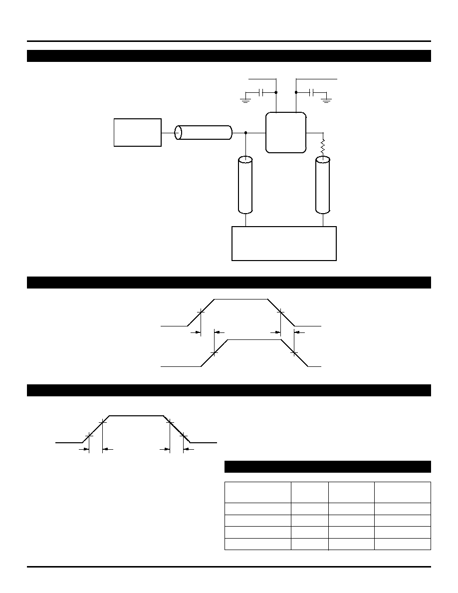
ECL/TTL WAVEFORMS: RISE AND FALL TIMES
V
OUT
T
rise
T
fall
2.0V
0.8V
LOGIC DIAGRAM
PRODUCT ORDERING CODE
Ordering
Package
Operating
Marking
Code
Type
Range
Code
SY10H641LC
J28-1
Commercial
SY10H641LC
SY10H641LJCTR*
J28-1
Commercial
SY10H641LC
SY100H641LJC
J28-1
Commercial
SY100H641LJC
SY100H641LJCTR*
J28-1
Commercial
SY100H641LJC
*Tape and Reel
5
ClockWorksTM
SY10H641L
SY100H641L
Micrel
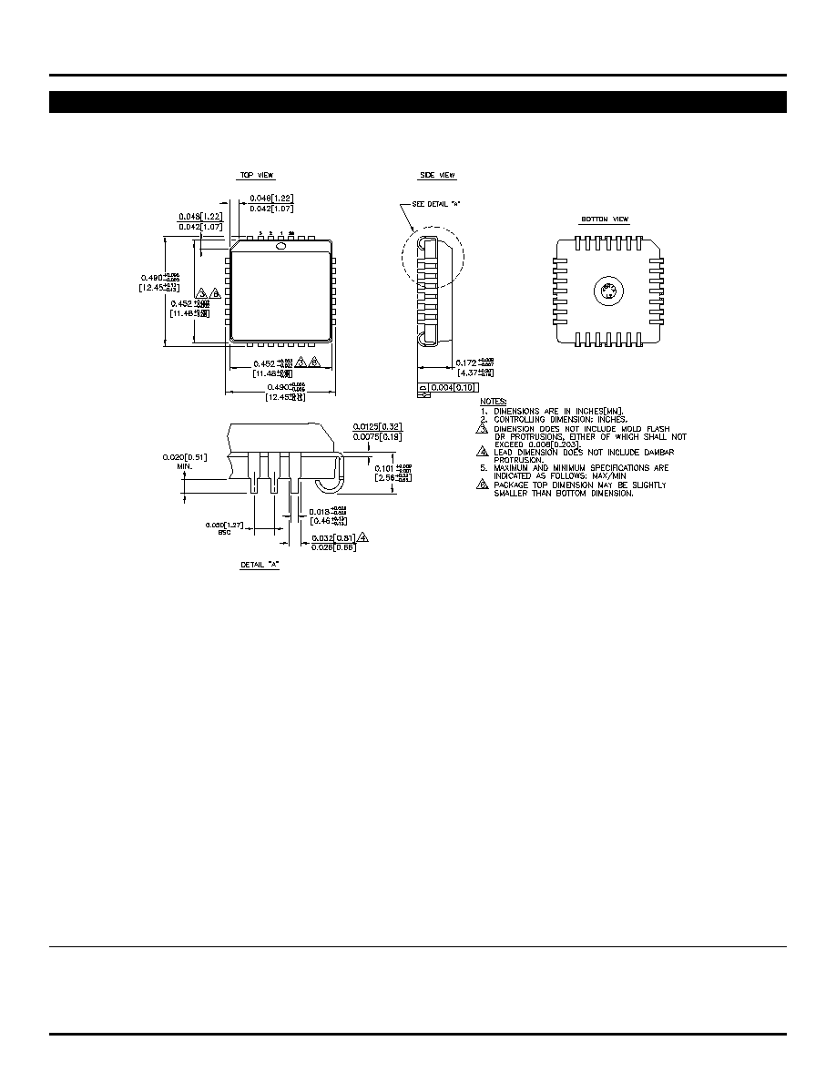
28 LEAD PLCC (J28-1)
Rev. 03
MICREL-SYNERGY
3250 SCOTT BOULEVARD
SANTA CLARA
CA 95054
USA
TEL
+ 1 (408) 980-9191
FAX
+ 1 (408) 914-7878
WEB
http://www.micrel.com
This information is believed to be accurate and reliable, however no responsibility is assumed by Micrel for its use nor for any infringement of patents or
other rights of third parties resulting from its use. No license is granted by implication or otherwise under any patent or patent right of Micrel Inc.
© 2002 Micrel Incorporated