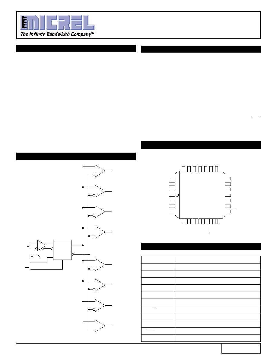
The SY100HA643 is an enhanced dual supply, low skew
translating 1:8 clock driver. Devices in the Micrel-Synergy
H600 translators series utilize the 28-lead PLCC for optimal
power pinning, signal flow through and electrical
performance. The dual-supply HA643 is similar to the H641,
which is a single-supply 1:9 version of the same function,
with higher performance than the H643 versions.
The device features a 48mA TTL output stage, with AC
performance specified into a 20pF load capacitance. A
Latch is provided on-chip. When LEN is LOW (or left open,
in which case it is pulled LOW by the internal pulldowns)
the latch is transparent. A HIGH on the enable pin (EN)
forces all outputs LOW.
The 100HA643 is compatible with 100K ECL logic levels.
DESCRIPTION
FEATURES
s
ECL/TTL version of popular ECLinPSTM E111
s
400ps within device skew
s
800ps part-to-part skew
s
Latch
s
Differential internal design
s
V
BB
output
s
Dual supply
s
Reset/Enable
s
Multiple TTL and ECL power/ground pins
s
Fully compatible with Motorola MC100H643
s
Higher performance than H643 versions
s
Industrial temperature availability
s
Available in 28-pin PLCC package
DUAL SUPPLY
OCTAL ECL-TO-TTL
Rev.: G
Amendment: /1
Issue Date: August, 1998
ClockWorksTM
SY100HA643
BLOCK DIAGRAM
PIN CONFIGURATION
Pin
Function
OGND
TTL Output Ground (0V)
OVTTTL
Output V
CC
(+5.0V)
IGND
Internal TTL GND (0V)
IVT
Internal TTL V
CC
(+5.0V)
V
EE
ECL V
EE
(-5.2/-4.5V)
V
CCE
ECL Ground (0V)
D, D
Signal Input (ECL)
V
BB
V
BB
Reference Output
Q0 - Q7
Signal Outputs (TTL)
EN
Enable Input (ECL)
LEN
Latch Enable Input (ECL)
PIN NAMES
D
V
BB
Q
0
Q
1
Q
2
Q
3
Q
4
Q
5
Q
6
Q
7
D
LEN
EN
D
Q
TTL OUTPUTS
18
17
16
15
14
13
12
5
6
7
8
9
10 11
SY100HA643
TOP VIEW
PLCC
Q
5
OVT
2
Q
6
OGND
4
Q
4
OGND
3
Q
7
Q
3
OGND
2
Q
2
OVT
1
Q
1
OGND
1
Q
0
1GND
1
V
EE
V
EE
EN
D
IVT
1
V
EE
V
CCE
V
CCE
LEN
V
BB
IVT
2
IGND
2
D
4
3
2
1
28
27
26
25 24
23 22 21 20 19
1
3
ClockWorksTM
SY100HA643
Micrel
AC CHARACTERISTICS
IVT = OVT = 5.0V
±
5%; V
EE
= ≠4.2V to ≠5.5V ; V
CCE
= GND
T
A
= ≠40
∞
C
T
A
= 0
∞
C
T
A
= +25
∞
C
T
A
= +85
∞
C
Symbol
Parameter
Min.
Max.
Min.
Max.
Min.
Max.
Min.
Max.
Unit
Condition
I
IH
Propagation Delay
D
to Output
LEN
2.3
3.1
2.3
3.1
2.3
3.1
2.3
3.1
ns
C
L
= 20pF
EN
t
skew
Within-Device Skew
(1)
--
0.4
--
0.4
--
0.4
--
0.4
ns
t
PW
Pulse Width Out
(2)
HIGH or LOW
4.5
5.5
4.5
5.5
4.5
5.5
4.5
5.5
ns
C
L
= 20pF
@ FOUT = 100MHz
t
S
Setup Time
D
0.75
--
0.75
--
0.75
--
0.75
--
ns
t
H
Hold Time
D
0.75
--
0.75
--
0.75
--
0.75
--
ns
t
RR
Recovery TimeLEN
1.25
--
1.25
--
1.25
--
1.25
--
ns
EN
1.25
--
1.25
--
1.25
--
1.25
--
ns
t
PW
Minimum PulseLEN
1.5
--
1.5
--
1.5
--
1.5
--
ns
Width
EN
1.5
--
1.5
--
1.5
--
1.5
--
ns
tr
Rise / Fall times
tf
0.8V -- 2.0V
--
1.5
--
1.5
--
1.5
--
1.5
ns
C
L
= 20pF
f
MAX
Max. Input Frequency
(3,4)
160
--
160
--
160
--
160
--
MHz
C
L
= 20pF
NOTES:
1. Within-Device skew defined as identical transitions on similar paths through a device.
2. Pulse width is defined relative to 1.5V measurement points on the output waveform.
3. Frequency at which output levels will meet a 0.8V to 2.0V minimum swing.
4. The f
MAX
value is specified as the minimum guaranteed maximum frequency. Actual operational maximum frequency may be greater.
Ordering
Package
Operating
Code
Type
Range
SY100HA643JC
J28-1
Commercial
SY100HA643JCTR
J28-1
Commercial
PRODUCT ORDERING CODE
Ordering
Package
Operating
Code
Type
Range
SY100HA643JI
J28-1
Industrial
SY100HA643JITR
J28-1
Industrial
4
ClockWorksTM
SY100HA643
Micrel
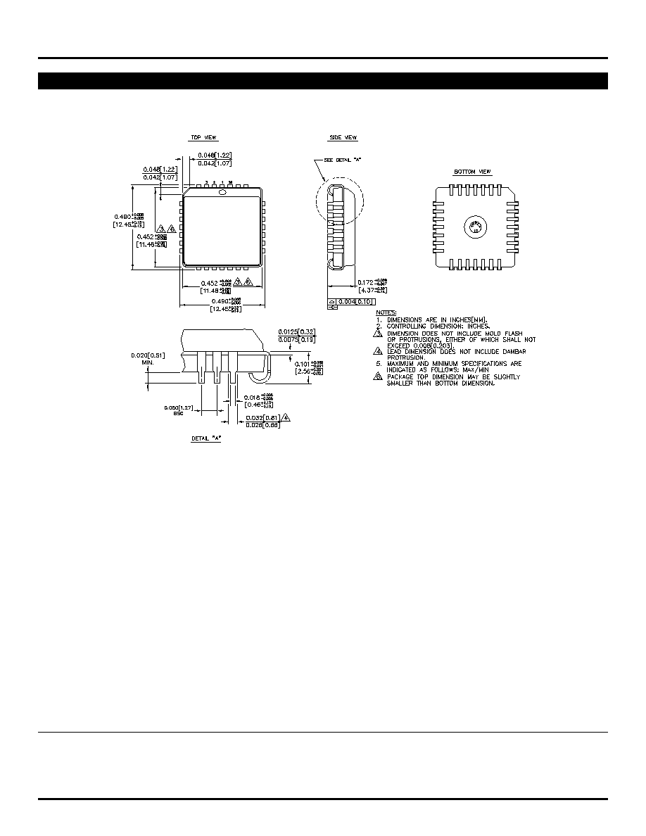
28 LEAD PLCC (J28-1)
Rev. 03
MICREL-SYNERGY
3250 SCOTT BOULEVARD
SANTA CLARA
CA 95054
USA
TEL
+ 1 (408) 980-9191
FAX
+ 1 (408) 914-7878
WEB
http://www.micrel.com
This information is believed to be accurate and reliable, however no responsibility is assumed by Micrel for its use nor for any infringement of patents or
other rights of third parties resulting from its use. No license is granted by implication or otherwise under any patent or patent right of Micrel Inc.
© 2000 Micrel Incorporated