LOW-POWER HEX
ECL-to-TTL
TRANSLATOR
DESCRIPTION
FEATURES
s
Max. propagation delay of 3.7ns
s
I
EE
min. of ≠37mA
s
TTL outputs
s
Extended supply voltage option:
V
EE
= ≠4.2V to ≠5.5V
s
25% faster than National's 325
s
Differential inputs with built-in offset
s
Voltage and temperature compensation for improved
noise immunity
s
V
BB
output for single-ended use
s
Internal 75K
input pull-down resistors
s
Function and pinout compatible with Fairchild F100K
s
Available in 24-pin CERPACK and 28-pin PLCC
packages
The SY100S325 are hex translators for converting
100K ECL logic levels to TTL logic levels. Inputs can be
used as inverting, non-inverting or differential receivers.
An internal reference voltage generator provides V
BB
for
single-ended operation or for use in Schmitt trigger
applications. All inputs have 75K
pull-down resistors.
The outputs will go LOW when the inputs are either open
or have the same potential.
When used in single-ended operation, the apparent
input threshold of the true inputs is 20mV to 40mV higher
(positive) than the threshold of the complementary inputs.
The V
TTL
and V
EE
power may be applied in either order.
SY100S325
PIN NAMES
Pin
Function
D
0
≠D
5
Data Inputs
D
0
≠D
5
Inverting Data Inputs
Q
0
≠Q
5
Data Outputs
V
EES
V
EE
Substrate
V
TTL
TTL V
CC
Power Supply
V
CCA
V
CCO
for ECL Outputs
18
17
16
15
14
13
12
5
6
7
8
9
10
11
2
3
4
1
Top View
Flatpack
F24-1
24
23
22
21
20
19
V
CC
V
CC
Q
1
V
TTL
Q
2
V
TTL
D
5
Q
4
Q
5
Q
3
D
4
D
5
Q
0
D
0
D
1
D
0
D
1
D
2
D
3
V
EE
V
B
B
D
4
D
2
D
3
Rev.: F
Amendment: /0
Issue Date:
July, 1999
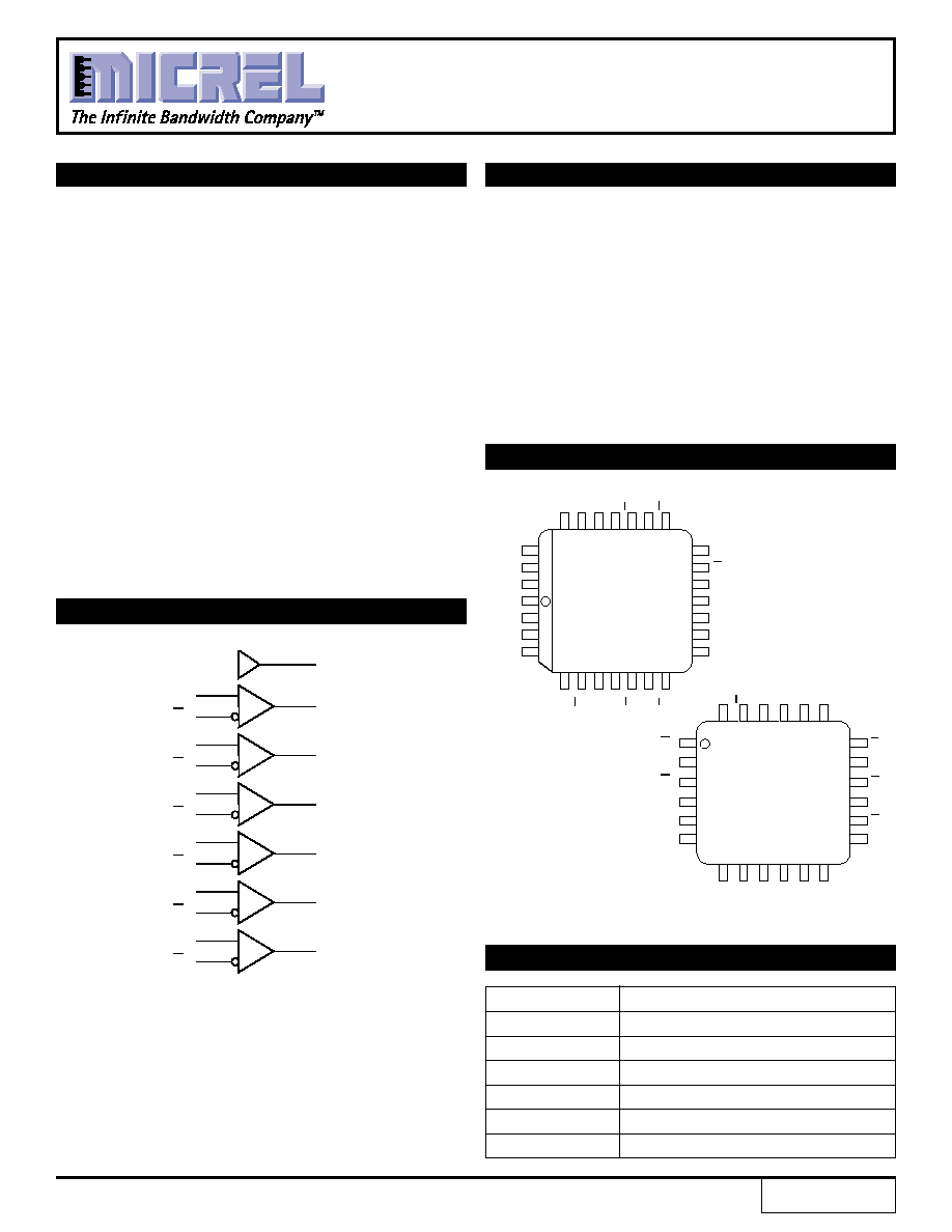
PIN CONFIGURATIONS
18
17
16
15
14
13
12
5
6
7
8
9
10 11
26
27
28
1
2
3
4
Top View
PLCC
J28-1
25 24 23 22 21 20 19
V
TTL
V
CC
V
CC
V
CC
Q
2
Q
1
V
TTL
D
0
V
EES
D
1
Q
0
D
0
D
1
D
2
D
4
D
3
V
EES
V
EE
V
BB
D
2
D
3
V
EES
D
5
Q
4
Q
3
Q
5
D
4
D
5
BLOCK DIAGRAM
D
0
Q
0
D
0
D
1
Q
1
D
1
D
2
Q
2
D
2
D
3
Q
3
D
3
D
4
Q
4
D
4
D
5
Q
5
D
5
V
BB
1
2
SY100S325
Micrel
AC ELECTRICAL CHARACTERISTICS
PLCC/FLATPACK
V
EE
= ≠4.2V to ≠5.5V unless otherwise specified, V
CC
= V
CCA
= GND, V
TTL
= +4.5V to +5.5V
Symbol
Parameter
Min.
Typ.
Max.
Unit
Condition
t
PLH
Propagation Delay
900
2100
2900
ps
C
L
= 15pF, Figure 2
t
PHL
Data to Output
t
PLH
Propagation Delay
900
3100
3700
ps
C
L
= 50pF, Figure 2
t
PHL
Data to Output
DC ELECTRICAL CHARACTERISTICS
V
EE
= ≠4.2V to ≠4.8V unless otherwise specified, V
CC
=V
CCA
= GND, V
TTL
= +4.5V to +5.5V
Symbol
Parameter
Min.
Typ.
Max.
Unit
Condition
V
OH
Output HIGH Voltage
2.5
--
--
V
I
OH
= ≠2.0mA
V
IN
= V
IH
(Max.)
V
OL
Output LOW Voltage
--
--
0.5
V
I
OL
= 24mA
V
IN
= V
IL
(Min.)
V
DIFF
Input Voltage Differential
150
--
--
mV
Required for Full Output Swing
V
CM
Common Mode Voltage
--
--
1.0
V
Permissible
±
V
CM
with Respect to V
BB
I
IH
Input HIGH Current
--
--
350
µ
A
V
IN
= V
IH
(Max.), D
0
≠D
5
= V
BB
, D
0
≠D
5
= V
IL
(Min.)
I
IL
Input LOW Current
0.5
--
--
µ
A
V
IN
= V
IH
(Min.), D
0
≠D
5
= V
BB
I
OS
Output Short Circuit Current
≠150
≠80
≠60
mA
V
OUT
= GND
I
EE
V
EE
Power Supply Current
≠37
≠24
≠17
mA
D
0
≠D
5
= V
BB
I
TTL
V
TTL
Power Supply Current
--
42
65
mA
D
0
≠D
5
= V
BB
V
BB
Ouptut Reference Voltage
≠1380
≠1320 ≠1260
mV
I
VBB
= ≠2.1mA
V
IH
Single-Ended Input HIGH
≠1165
--
≠880
mV
Guaranteed HIGH Signal for All Inputs (with One
Voltage
Tied to V
BB
)
V
IL
Single-Ended Input LOW
≠1810
--
≠1475
mV
Guaranteed LOW Signal for All Inputs (with One
Voltage
Tied to V
BB
)
3
SY100S325
Micrel
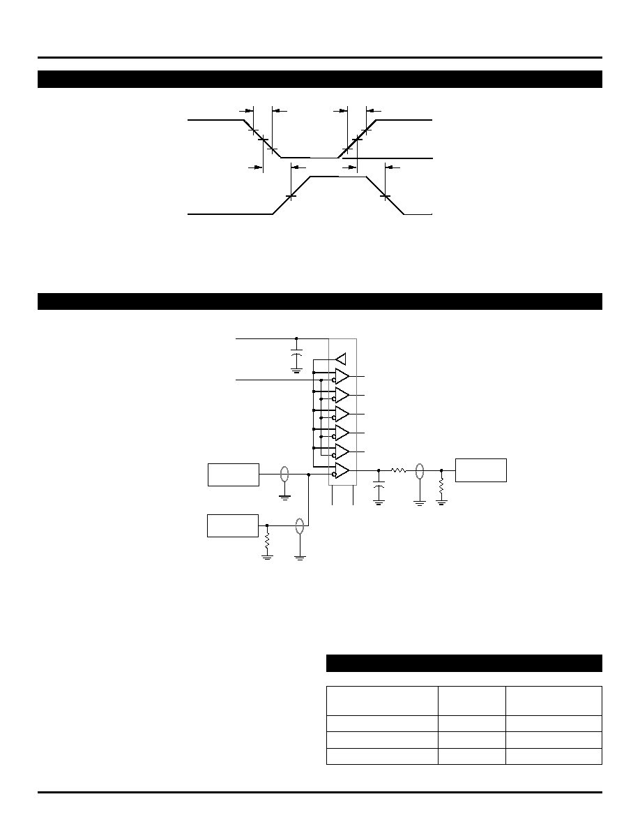
SWITCHING WAVEFORM
Figure 1. Propagation Delay
t
PLH
INPUT
ATTENUATED
OUTPUT
50%
0.7
±
0.1 ns
0.7
±
0.1 ns
≠0.95V
20%
80%
50%
≠1.69V
t
PHL
TEST CIRCUITS
SCOPE
CHAN B
V
BB
V
TTL
V
EE
V
CC
0.1
µ
F
OPEN
R
T
C
L
R
T
450
L2
PULSE
GENERATOR
SCOPE
CHAN A
L1
Figure 2. AC Test Circuit for 15pF Loading
NOTES:
V
CC
= 0V, V
EE
= ≠4.5V, V
TTL
= +5V
L1 and L2 = equal length 50
impedance lines
R
T
= 50
terminator internal to scope
Decoupling 0.1
µ
F from GND to V
CC
, V
EE
and V
TTL
All unused outputs are loaded with 500
to GND
C
L
= Fixture and stray capacitance = 3pF
PRODUCT ORDERING CODE
Ordering
Package
Operating
Code
Type
Range
SY100S325FC
F24-1
Commercial
SY100S325JC
J28-1
Commercial
SY100S325JCTR
J28-1
Commercial
NOTE:
V
EE
= ≠4.2V to ≠5.5V unless otherwise specified, V
CC
= V
CCA
= GND
5
SY100S325
Micrel
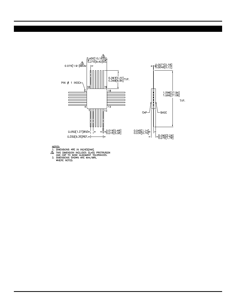
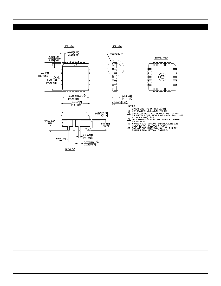
28 LEAD PLCC (J28-1)
Rev. 03
MICREL-SYNERGY
3250 SCOTT BOULEVARD
SANTA CLARA
CA 95054
USA
TEL
+ 1 (408) 980-9191
FAX
+ 1 (408) 914-7878
WEB
http://www.micrel.com
This information is believed to be accurate and reliable, however no responsibility is assumed by Micrel for its use nor for any infringement of patents or
other rights of third parties resulting from its use. No license is granted by implication or otherwise under any patent or patent right of Micrel Inc.
© 2000 Micrel Incorporated