Pin
Function
CP
Clock Pulse Input
CEP
Count Enable Parallel Input (Active LOW)
D
0
/CET
Serial Data Input/Count Enable Trickle
Input (Active LOW)
S
0
-- S
2
Select Inputs
MR
Master Reset Input
V
EES
V
EE
Substrate
V
CCA
V
CCO
for ECL Outputs
P
0
≠ P
3
Preset Inputs
D
3
Serial Data Input
TC
Terminal Count Output
Q
0
-- Q
3
Data Outputs
Q
0
-- Q
3
Complementary Data Outputs
PIN NAMES
SY100S336
4-STAGE COUNTER/
SHIFT REGISTER
s
Max. shift frequency of 700MHz
s
Clock to Q delay max. of 1100ps
s
I
EE
min. of ≠170mA
s
Internal 75K
input pull-down resistors
s
Industry standard 100K ECL levels
s
Extended supply voltage option:
V
EE
= ≠4.2V to ≠5.5V
s
Voltage and temperature compensation for improved
noise immunity
s
50% faster than Fairchild 300K at lower power
s
Function and pinout compatible with Fairchild F100K
s
Available in 24-pin CERPACK and 28-pin PLCC
packages
FEATURES
DESCRIPTION
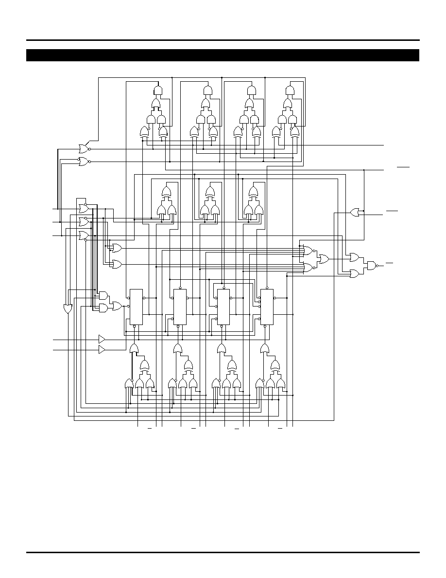
The SY100S336 functions either as a modulo-16 up/
down counter or as a 4-bit bidirectional shift register and is
designed for use in high-performance ECL systems. Three
Select inputs (Sn) are provided for determining the mode of
operation. The Function Table lists the available modes of
operation. In order to allow cascading for multistage
counters, two Count Enable controls (CEP, CET) are
provided. The CET input also functions as the Serial Data
input (S
0
) for a shift-up operation, while the D
3
input serves
as the Serial Data input for the shift-down operation.
When the device is in the counting mode, the Terminal
Count (TC) goes to a logical LOW when the count reaches
15 for count-up or reaches 0 for count-down. When in the
shift mode, the TC output simply repeats the Q
3
output.
The flexiblity provided by the TC/Q
3
output and the D
0
/
CET input allows these signals to be interconnected from
one stage to the next higher stage for multistage counting
or shift-up operations. The individual Presets (P
n
) allow
initialization of the counter by entering data in parallel to
preset the counter. A logic HIGH on the Master Reset (MR)
overrides all other inputs and asynchronously clears the
flip-flops. An additional synchronous Clear is provided, as
well as a complement function which synchronously inverts
the contents of the flip-flops. All inputs have 75K
pull-
down resistors.
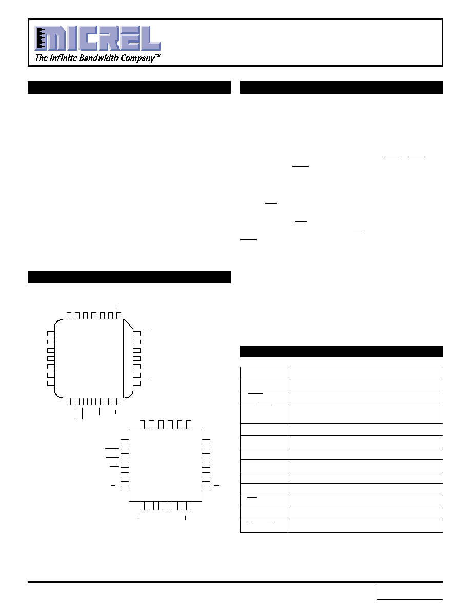
PIN CONFIGURATIONS
Q
2
Q
2
V
CCA
V
CC
Q
1
V
CC
P
0
V
EE
MR
CP
S
0
V
EES
4
3
2
1
28
27
12
13
14
15
16
17
19
11
20
10
21
9
22
8
23
7
24
6
Top View
PLCC
J28-1
Q
1
S
1
26
18
25
5
P
1
P
2
P
3
V
EES
D
3
Q
3
Q
3
D
0
/CET
V
EES
CEP
TC
S
2
Q
0
Q
0
S
1
S
0
M
R
V
EE
CP
P
0
P
1
P
2
P
3
D
3
Q
3
Q
3
S
2
D
0
/CET
Q
0
CEP
Q
0
TC
18
17
16
15
14
13
1
2
3
4
5
6
7
24
8
23
9
22
10
21
11
20
12
19
Top View
Flatpack
F24-1
V
CC
V
CCA
Q
1
Q
2
Q
1
Q
2
Rev.: G
Amendment: /0
Issue Date:
July, 1999
1
3
SY100S336
Micrel
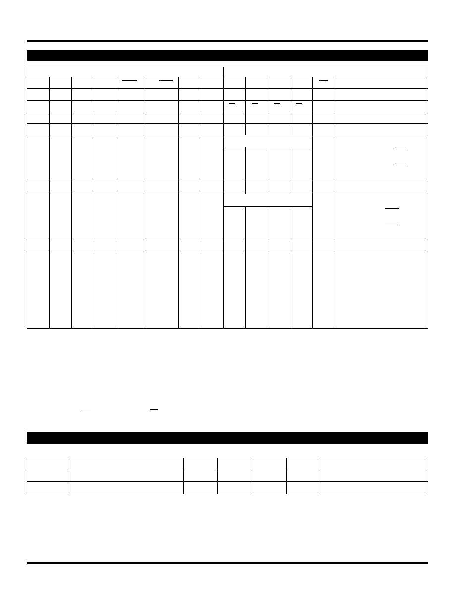
Inputs
Outputs
MR
S
2
S
1
S
0
CEP
D
0
/CET
D
3
CP
Q
0
Q
1
Q
2
Q
3
TC
Mode
L
L
L
L
X
X
X
u
P
0
P
1
P
2
P
3
L
Preset (Parallel Load)
L
L
L
H
X
X
X
u
Q
0
Q
1
Q
2
Q
3
L
Invert
L
L
H
L
X
X
X
u
Q
1
Q
2
Q
3
D
3
D
3
Shift Left
L
L
H
H
X
X
X
u
D
0
Q
0
Q
1
Q
2
Q
3
*
Shift Right
L
H
L
L
L
L
X
u
(Q
0≠3
) minus 1
x
Count Down
L
H
L
L
H
L
X
X
Q
0
Q
1
Q
2
Q
3
x
Count Down with CEP
Not Active
L
H
L
L
X
H
X
X
Q
0
Q
1
Q
2
Q
3
H
Count Down with CET
Not Active
L
H
L
H
X
X
X
u
L
L
L
L
H
Clear
L
H
H
L
L
L
X
u
(Q
0≠3
) plus 1
Count Up
L
H
H
L
H
L
X
X
Q
0
Q
1
Q
2
Q
3
Count Up with CEP
Not Active
L
H
H
L
X
H
X
X
Q
0
Q
1
Q
2
Q
3
H
Count Up with CET
Not Active
L
H
H
H
X
X
X
X
Q
0
Q
1
Q
2
Q
3
H
Hold
H
L
L
L
X
X
X
X
L
L
L
L
L
Asynchronous Master
H
L
L
H
X
X
X
X
L
L
L
L
L
Reset
H
L
H
L
X
X
X
X
L
L
L
L
L
H
L
H
H
X
X
X
X
L
L
L
L
L
H
H
L
L
X
L
X
X
L
L
L
L
L
H
H
L
L
X
H
X
X
L
L
L
L
H
H
H
L
H
X
X
X
X
L
L
L
L
H
H
H
H
L
X
X
X
X
L
L
L
L
H
H
H
H
H
X
X
X
X
L
L
L
L
H
TRUTH TABLE
(1)
NOTE:
1. H = High Voltage Level
L = Low Voltage Level
X = Don't Care
u = LOW-to-HIGH Transition
x
= L if Q
0
≠ Q
3
= LLLL
H if Q
0
≠ Q
3
LLLL
= L if Q
0
≠ Q
3
= HHHH
H if Q
0
≠ Q
3
HHHH
* Before the clock, TC is Q
3
; after the clock, TC is Q
2
DC ELECTRICAL CHARACTERISTICS
V
EE
= ≠4.2V to ≠5.5V unless otherwise specified, V
CC
= V
CCA
= GND
Symbol
Parameter
Min.
Typ.
Max.
Unit
Condition
I
IH
Input HIGH Current, All Inputs
--
--
200
µ
A
V
IN
= V
IH
(Max.)
I
EE
Power Supply Current
≠170
≠145
≠90
mA
Inputs Open