Label
Function
CP
Clock Pulse Input
S
0
-- S
1
Select Inputs
D
0
-- D
7
Serial Inputs
P
0
-- P
7
Parallel Inputs
Q
0
-- Q
7
Data Outputs
V
EES
V
EE
Substrate
V
CCA
V
CCO
for ECL Outputs
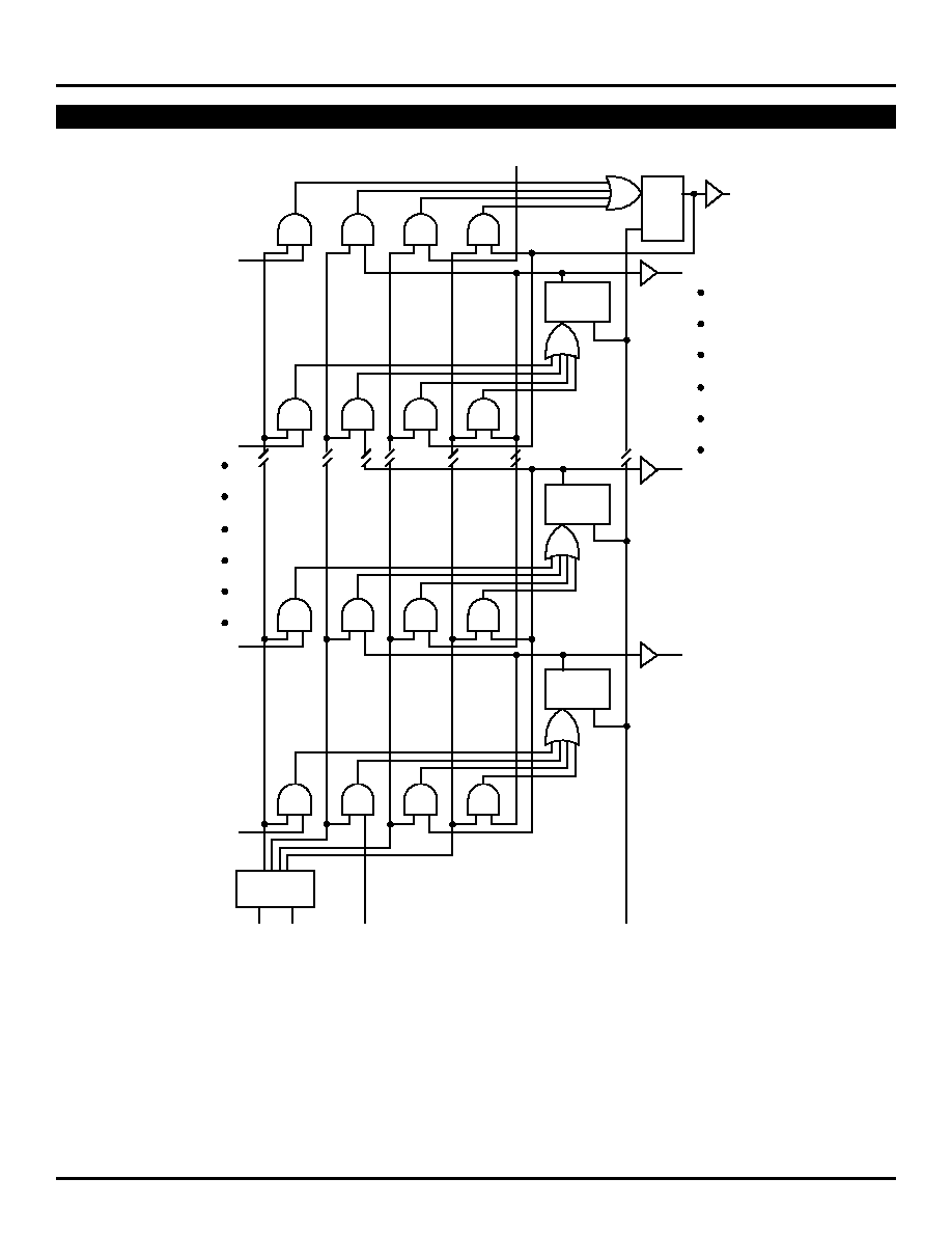
SY100S341
8-BIT SHIFT
REGISTER
s
Max. shift frequency of 600MHz
s
Max. Clock to Q delay of 1200ps
s
I
EE
min. of ≠150mA
s
Industry standard 100K ECL levels
s
Extended supply voltage option:
V
EE
= ≠4.2V to ≠5.5V
s
Voltage and temperature compensation for improved
noise immunity
s
Internal 75K
input pull-down resistors
s
70% faster than Fairchild 300K at lower power
s
Function and pinout compatible with Fairchild F100K
s
Available in 24-pin CERPACK and 28-pin PLCC
packages
FEATURES
DESCRIPTION
The SY100S341 offer eight D-type, edge-triggered flip-
flops with both individual inputs for parallel operation as
well as serial inputs for bidirectional shifting, and are
designed for use in high-performance ECL systems. Data
is clocked into the flip-flops on the rising edge of the clock.
The mode of operation is selected by two Select inputs
(S
0
, S
1
) which determine if the device performs a shift, hold
or parallel entry function, as described in the Truth Table.
The inputs on these devices have 75K
pull-down resistors.
PIN NAMES
PIN CONFIGURATIONS
P
3
S
1
S
0
V
EE
CP
P
4
P
5
P
6
P
7
D
7
Q
8
Q
7
P
2
P
0
Q
0
P
1
Q
1
D
0
18
17
16
15
14
13
1
2
3
4
5
6
7
24
8
23
9
22
10
21
11
20
12
19
Top View
Flatpack
F24-1
V
CC
V
CCA
Q
3
Q
4
Q
2
Q
5
Rev.: G
Amendment: /0
Issue Date:
July, 1999
Q
5
Q
4
V
CCA
V
CC
Q
3
V
CC
P
4
V
EE
S
0
CP
S
1
V
EES
4
3
2
1
28
27
12
13
14
15
16
17
19
11
20
10
21
9
22
8
23
7
24
6
Top View
PLCC
J28-1
Q
2
P
3
26
18
25
5
P
5
P
6
P
7
V
EES
D
7
Q
7
Q
6
P
0
V
EES
P
1
D
0
P
2
Q
0
Q
1
1
3
SY100S341
Micrel
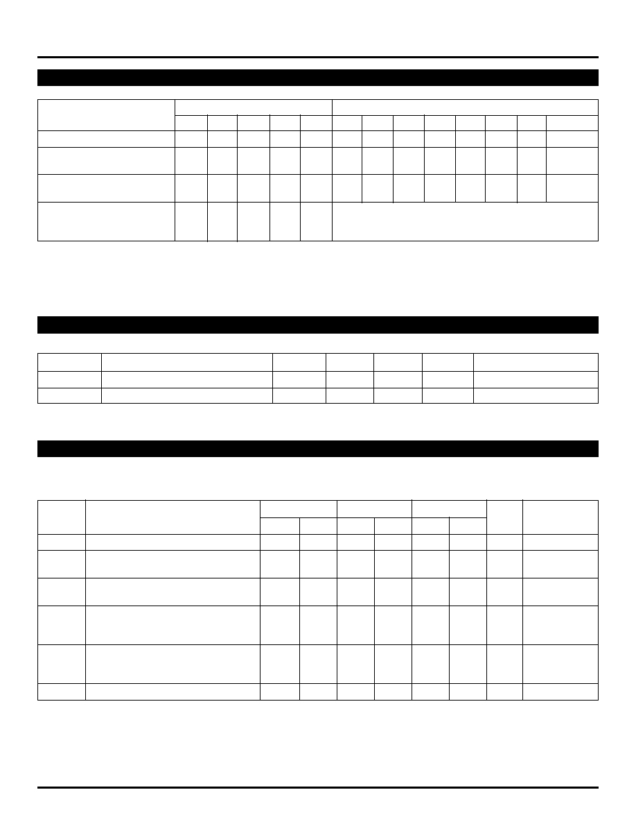
TRUTH TABLE
NOTE:
1. H = HIGH Voltage Level
L = LOW Voltage Level
X = Don't Care
u = LOW-to-HIGH Transition
DC ELECTRICAL CHARACTERISTICS
V
EE
= ≠4.2V to ≠5.5V unless otherwise specified; V
CC
= V
CCA
= GND
Inputs
Outputs
Function
D
7
D
0
S
1
S
0
CP
Q
7
Q
6
Q
5
Q
4
Q
3
Q
2
Q
1
Q
0
Load Register
X
X
L
L
u
P
7
P
6
P
5
P
4
P
3
P
2
P
1
P
0
Shift Left
X
L
L
H
u
Q
6
Q
5
Q
4
Q
3
Q
2
Q
1
Q
0
L
Shift Left
X
H
L
H
u
Q
6
Q
5
Q
4
Q
3
Q
2
Q
1
Q
0
H
Shift Right
L
X
H
L
u
L
Q
7
Q
6
Q
5
Q
4
Q
3
Q
2
Q
1
Shift Right
H
X
H
L
u
H
Q
7
Q
6
Q
5
Q
4
Q
3
Q
2
Q
1
Hold
X
X
H
H
X
No Change
Hold
X
X
X
X
H
Hold
X
X
X
X
L
Symbol
Parameter
Min.
Typ.
Max.
Unit
Condition
I
IH
Input HIGH Current, All Inputs
--
--
200
µ
A
V
IN
= V
IH
(Max.)
I
EE
Power Supply Current
≠150
≠102
≠71
mA
Inputs Open
AC ELECTRICAL CHARACTERISTICS
CERPACK
V
EE
= ≠4.2V to ≠5.5V unless otherwise specified; V
CC
= V
CCA
= GND
T
A
= 0
∞
C
T
A
= +25
∞
C
T
A
= +85
∞
C
Symbol
Parameter
Min.
Max.
Min.
Max.
Min.
Max.
Unit
Condition
f
shift
Shift Frequency
600
--
600
--
600
--
MHz
t
PLH
Propagation Delay
450
1200
450
1200
450
1200
ps
t
PHL
CP to Output
t
TLH
Transition Time
300
900
300
900
300
900
ps
t
THL
20% to 80%, 80% to 20%
t
S
Set-up Time
ps
D
n
, P
n
300
--
300
--
300
--
S
n
600
--
600
--
600
--
t
H
Hold Time
ps
D
n
, P
n
300
--
300
--
300
--
S
n
0
--
0
--
0
--
t
pw
(H)
Pulse Width HIGH, CP
--
600
--
600
--
600
ps

4
SY100S341
Micrel
AC ELECTRICAL CHARACTERISTICS
PLCC
V
EE
= ≠4.2V to ≠5.5V unless otherwise specified; V
CC
= V
CCA
= GND
T
A
= 0
∞
C
T
A
= +25
∞
C
T
A
= +85
∞
C
Symbol
Parameter
Min.
Max.
Min.
Max.
Min.
Max.
Unit
Condition
f
shift
Shift Frequency
600
--
600
--
600
--
MHz
t
PLH
Propagation Delay
450
1200
450
1200
450
1200
ps
t
PHL
CP to Output
t
TLH
Transition Time
300
900
300
900
300
900
ps
t
THL
20% to 80%, 80% to 20%
t
S
Set-up Time
ps
D
n
, P
n
300
--
300
--
300
--
S
n
600
--
600
--
600
--
t
H
Hold Time
ps
D
n
, P
n
300
--
300
--
300
--
S
n
0
--
0
--
0
--
t
pw
(H)
Pulse Width HIGH, CP
--
600
--
600
--
600
ps
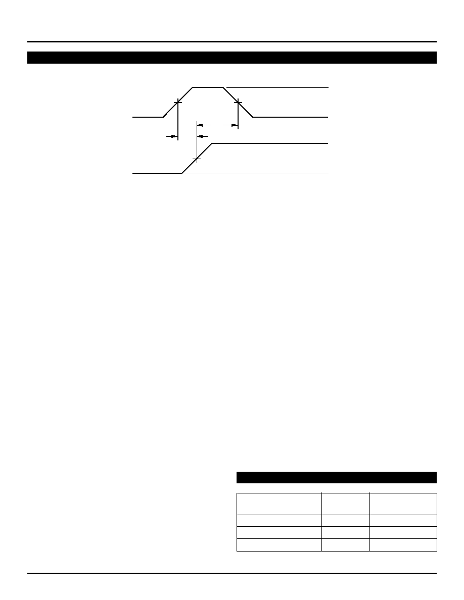
TIMING DIAGRAMS
Propagation Delay and Transition Times
PARALLEL
20%
80%
50%
t
PLH
t
PHL
t
TLH
t
THL
0.7
±
0.1 ns
0.7
±
0.1 ns
≠0.95V
≠1.69V
CLOCK
OUTPUT
1/fshift
tpw (H)
≠0.95V
≠1.69V
5
SY100S341
Micrel
TIMING DIAGRAMS
Set-up and Hold Times
NOTES:
1. V
EE
= ≠4.2V to ≠5.5V unless otherwise specified; V
CC
= V
CCA
= GND.
2. t
S
is the minimum time before the transition of the clock that information must be present at the data input.
3. t
H
is the minimum time after the transition of the clock that information must remain unchanged at the data input.
Ordering
Package
Operating
Code
Type
Range
SY100S341FC
F24-1
Commercial
SY100S341JC
J28-1
Commercial
SY100S341JCTR
J28-1
Commercial
PRODUCT ORDERING CODE
CLOCK
50%
≠1.69V
P
n
, S
n
, D
n
t
S
50%
t
H
≠0.95V
≠1.69V
≠0.95V