
BLOCK DIAGRAM
D
R
D
5
Q
5
E
Q
5
D
R
D
4
Q
4
E
Q
4
D
R
D
3
Q
3
E
Q
3
D
R
D
2
Q
2
E
Q
2
D
R
D
1
Q
1
E
Q
1
D
R
D
0
Q
0
E
Q
0
CP
b
MR
CP
a
Q
Q
Q
Q
Q
Q
Q
Q
Q
Q
Q
Q
s
Max. toggle frequency of 700MHz
s
Clock to Q max. of 1200ps
s
I
EE
min. of ≠98mA
s
Industry standard 100K ECL levels
s
Extended supply voltage option:
V
EE
= ≠4.2V to ≠5.5V
s
Voltage and temperature compensation for improved
noise immunity
s
Internal 75K
input pull-down resistors
s
50% faster than Fairchild 300K
s
Better than 20% lower power than Fairchild
s
Function and pinout compatible with Fairchild F100K
s
Available in 24-pin CERPACK and 28-pin PLCC
packages
FEATURES
HEX D FLIP-FLOP
SY100S351
DESCRIPTION
The SY100S351 offers six D-type, edge-triggered,
master/slave flip-flops with differential outputs, and is
designed for use in high-performance ECL systems. The
flip-flops are controlled by the signal from the logical OR
operation on a pair of common clock signals (CP
a
, CP
b
).
Data enters the master when both CP
a
and CP
b
are LOW
and transfers to the slave when either CP
a
or CP
b
(or both)
go to a logic HIGH. The Master Reset (MR) input overrides
all other inputs and takes the Q outputs to a logic LOW. The
inputs on this device have 75K
pull-down resistors.
Rev.: G
Amendment: /0
Issue Date:
July, 1999
CP
b
CP
a
MR
V
EE
D
3
D
2
D
1
D
0
Q
0
Q
0
Q
1
Q
1
D
4
Q
5
Q
4
D
5
Q
4
Q
5
18
17
16
15
14
13
1
2
3
4
5
6
7
24
8
23
9
22
10
21
11
20
12
19
Top View
Flatpack
F24-1
V
CC
V
CCA
Q
3
Q
2
Q
3
Q
2
Q
2
Q
2
V
CCA
V
CC
Q
3
V
CC
D
2
V
EE
MR
D
3
CP
a
V
EES
4
3
2
1
28
27
12
13
14
15
16
17
19
11
20
10
21
9
22
8
23
7
24
6
Top View
PLCC
J28-1
Q
3
CP
b
26
18
25
5
D
1
D
0
Q
0
V
EES
Q
0
Q
1
Q
1
Q
5
V
EES
D
5
Q
5
D
4
Q
4
Q
4
PIN CONFIGURATIONS
1

2
SY100S351
Micrel
TRUTH TABLES
Asynchronous Operation
(1)
Inputs
Outputs
D
n
CP
a
CP
b
MR
Q
n
(t+1)
X
X
X
H
L
NOTE:
1. H = High Voltage Level
L = Low Voltage Level
X = Don't Care
t = Time before CP Positive Transition
t+1 = Time after CP Positive Transition
u = LOW-to-HIGH Transition
Synchronous Operation
(1)
Inputs
Outputs
D
n
CP
a
CP
b
MR
Q
n
(t+1)
L
u
L
L
L
H
u
L
L
H
L
L
u
L
L
H
L
u
L
H
X
H
u
L
Q
n
(t)
X
u
H
L
Q
n
(t)
X
L
L
L
Q
n
(t)
Pin
Function
D
0
-- D
5
Data Inputs
CP
a
, CP
b
Common Clock Inputs
MR
Asynchronous Master Reset Input
Q
0
-- Q
5
Data Outputs
Q
0
-- Q
5
Complementary Data Outputs
V
EES
V
EE
Substrate
V
CCA
V
CCO
for ECL Outputs
PIN NAMES
DC ELECTRICAL CHARACTERISTICS
V
EE
= ≠4.2V to ≠5.5V unless otherwise specified; V
CC
= V
CCA
= GND
Symbol
Parameter
Min.
Typ.
Max.
Unit
Condition
I
IH
Input HIGH Current
µ
A
V
IN
= V
IH
(Max.)
MR
--
--
270
D
0
≠ D
5
--
--
200
CP
a
, CP
b
--
--
300
I
EE
Power Supply Current
≠98
≠71
≠49
mA
Inputs Open
3
SY100S351
Micrel
T
A
= 0
∞
C
T
A
= +25
∞
C
T
A
= +85
∞
C
Symbol
Parameter
Min.
Max.
Min.
Max.
Min.
Max.
Unit
Condition
f
MAX
Toggle Frequency
700
--
700
--
700
--
MHz
t
PLH
Propagation Delay
--
1200
--
1200
--
1200
ps
t
PHL
CP
a
, CP
b
to Output
t
PLH
Propagation Delay
--
1200
--
1200
--
1200
ps
t
PHL
MR to Output
t
TLH
Transition Time
300
900
300
900
300
900
ps
t
THL
20% to 80%, 80% to 20%
t
S
Set-up Time
ps
D
0
≠D
5
500
--
500
--
500
--
MR (Release Time)
1000
--
1000
--
1000
--
t
H
Hold Time, D
0
≠D
5
550
--
550
--
550
--
ps
t
PW
(H)
Pulse Width HIGH
1000
--
1000
--
1000
--
ps
CP
a
, CP
b
, MR
AC ELECTRICAL CHARACTERISTICS
CERPACK
V
EE
= ≠4.2V to ≠5.5V unless otherwise specified; V
CC
= V
CCA
= GND
T
A
= 0
∞
C
T
A
= +25
∞
C
T
A
= +85
∞
C
Symbol
Parameter
Min.
Max.
Min.
Max.
Min.
Max.
Unit
Condition
f
MAX
Toggle Frequency
700
--
700
--
700
--
MHz
t
PLH
Propagation Delay
--
1200
--
1200
--
1200
ps
t
PHL
CP
a
, CP
b
to Output
t
PLH
Propagation Delay
--
1200
--
1200
--
1200
ps
t
PHL
MR to Output
t
TLH
Transition Time
300
900
300
900
300
900
ps
t
THL
20% to 80%, 80% to 20%
t
S
Set-up Time
ps
D
0
≠D
5
500
--
500
--
500
--
MR (Release Time)
1000
--
1000
--
1000
--
t
H
Hold Time, D
0
≠D
5
550
--
550
--
550
--
ps
t
PW
(H)
Pulse Width HIGH
1000
--
1000
--
1000
--
ps
CP
a
, CP
b
, MR
PLCC
V
EE
= ≠4.2V to ≠5.5V unless otherwise specified; V
CC
= V
CCA
= GND
4
SY100S351
Micrel
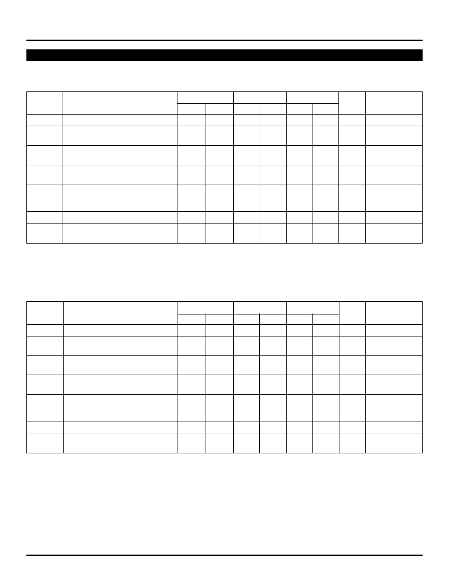
TIMING DIAGRAMS
Propagation Delay (Clock) and Transition Times
OUTPUT
DATA
20%
80%
50%
t
PLH
t
PHL
t
TLH
t
THL
0.7
±
0.1 ns
0.7
±
0.1 ns
≠0.95V
≠1.69V
CLOCK
OUTPUT
t
PHL
t
PLH
50%
1/fmax
tpw (H)
NOTE:
V
EE
= ≠4.2V to ≠5.5V unless otherwise specified; V
CC
= V
CCA
= GND
OUTPUT
MR
50%
t
PLH
t
PHL
≠1.69V
CLOCK
OUTPUT
t
PHL
t
PLH
50%
tpw (H)
20%
80%
50%
0.7
±
0.1 ns
0.7
±
0.1 ns
≠0.95V
t
S
(RELEASE TIME)
20%
80%
50%
Propagation Delay (Resets)

5
SY100S351
Micrel
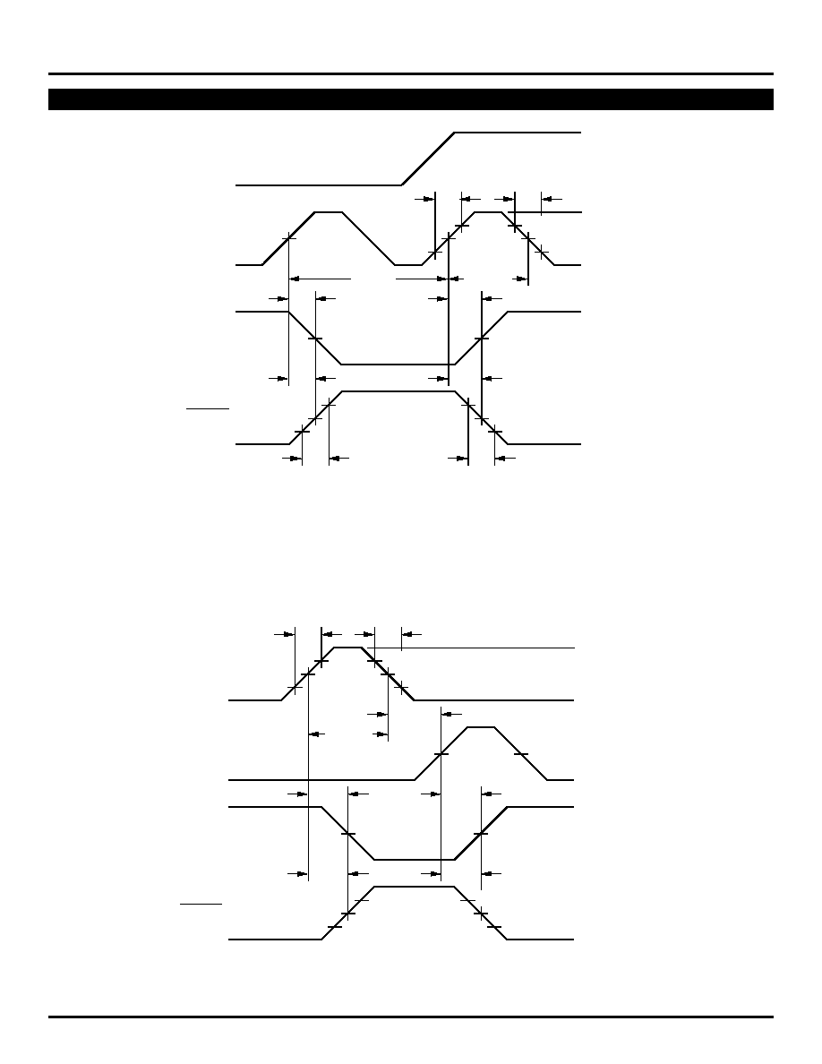
TIMING DIAGRAMS
Data Set-up and Hold Time
NOTES:
1. V
EE
= ≠4.2V to ≠5.5V unless otherwise specified; V
CC
= V
CCA
= GND
2. t
S
is the minimum time before the transition of the clock that information
must be present at the data input.
3. t
H
is the minimum time after the transition of the clock that information must
remain unchanged at the data input.
PRODUCT ORDERING CODE
Ordering
Package
Operating
Code
Type
Range
SY100S351FC
F24-1
Commercial
SY100S351JC
J28-1
Commercial
SY100S351JCTR
J28-1
Commercial
CLOCK
50%
≠1.69V
DATA
t
S
50%
t
H
≠0.95V
≠1.69V
≠0.95V