QUAD
MULTIPLEXER/LATCH
SY100S355
FEATURES
s
Max. propagation delay of 1100ps
s
Max. enable to output delay of 1400ps
s
I
EE
min. of ≠80mA
s
Industry standard 100K ECL levels
s
Extended supply voltage option:
V
EE
= ≠4.2V to ≠5.5V
s
Voltage and temperature compensation for improved
noise immunity
s
Internal 75K
input pull-down resistors
s
50% faster than Fairchild
s
Function and pinout compatible with Fairchild F100K
s
Available in 24-pin CERPACK and 28-pin PLCC
packages
DESCRIPTION
The SY100S355 offers four transparent latches with
differential outputs and is designed for use in high-
performance ECL systems. The Select inputs (S
0
, S
1
)
select one of the two sources of input data (D
0
or D
1
) to the
latch. The Select inputs can also force the outputs to a logic
LOW when the latch is in the transparent mode. The
latches are in the transparent mode when both Enables
(E
1
, E
2
) are at a logic LOW state. In the transparent mode,
the Select inputs can pass an input logic HIGH from D
0
or
D
1
to the output.
If the Select inputs are tied together, then input data from
either D
0
or D
1
is always passed through. A rising edge on
either Enable input will latch the outputs with the most
recent data at the latch inputs being stored. The Master
Reset (MR) input overrides all other inputs and takes the Q
outputs to a logic LOW. The inputs on this device have
75K
pull-down resistors.
Rev.: G
Amendment: /0
Issue Date:
July, 1999
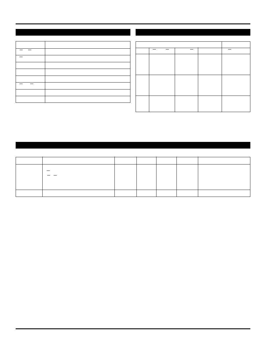
PIN CONFIGURATIONS
BLOCK DIAGRAM
D
CD
D
0a
Q
a
E
Q
a
Q
D
1a
D
CD
D
0b
Q
b
E
Q
b
Q
D
1b
D
CD
D
0c
Q
c
E
Q
c
Q
D
1c
D
CD
D
0d
Q
d
E
Q
d
Q
D
1d
MR
S
1
S
0
E
1
E
2
E
2
E
1
M
R
V
EE
S
1
S
0
D
1b
D
0b
D
1a
D
0a
Q
a
Q
a
D
0c
D
0d
Q
d
D
1c
Q
d
D
1d
18
17
16
15
14
13
1
2
3
4
5
6
7
24
8
23
9
22
10
21
11
20
12
19
Top View
Flatpack
F24-1
V
CC
V
CCA
Q
c
Q
b
Q
c
Q
b
Q
b
Q
b
V
CCA
V
CC
Q
c
V
CC
S
0
V
EE
MR
S
1
E
1
V
EES
4
3
2
1
28
27
12
13
14
15
16
17
19
11
20
10
21
9
22
8
23
7
24
6
Top View
PLCC
J28-1
Q
c
E
2
26
18
25
5
D
1b
D
0b
D
1a
V
EES
D
0a
Q
a
Q
a
D
0d
V
EES
D
1c
D
1d
D
0c
Q
d
Q
d
1
2
SY100S355
Micrel
Inputs
Outputs
MR
E
1
E
2
S
1
S
0
D
1X
D
0X
Q
X
Q
X
H
X
X
X
X
X
X
H
L
L
L
L
H
H
H
X
L
H
L
L
L
H
H
L
X
H
L
L
L
L
L
L
X
H
L
H
L
L
L
L
L
X
L
H
L
L
L
L
L
H
X
X
H
L
L
L
L
H
L
H
X
L
H
L
L
L
H
L
X
H
L
H
L
L
L
H
L
L
L
H
L
L
H
X
X
X
X
X
Latched
L
X
H
X
X
X
X
Latched
NOTE:
1. H = High Voltage Level
L = Low Voltage Level
X = Don't Care
TRUTH TABLE
(1)
DC ELECTRICAL CHARACTERISTICS
V
EE
= ≠4.2V to ≠5.5V unless otherwise specified; V
CC
= V
CCA
= GND
Symbol
Parameter
Min.
Typ.
Max.
Unit
Condition
I
IH
Input HIGH Current
µ
A
V
IN
= V
IH
(Max.)
S
0
, S
1
--
--
220
E
1
, E
2
--
--
350
D
na
, D
nd
--
--
340
MR
--
--
430
I
EE
Power Supply Current
≠80
≠57
≠40
mA
Inputs Open
Pin
Function
E
1
≠ E
2
Enable Inputs (Active LOW)
S
0
, S
1
Select Inputs
MR
Master Reset
D
na
≠ D
nd
Data Inputs
Q
a
≠ Q
d
Data Outputs
Q
a
-- Q
d
Complementary Data Outputs
V
EES
V
EE
Substrate
V
CCA
V
CCO
for ECL Outputs
PIN NAMES
3
SY100S355
Micrel
T
A
= 0
∞
C
T
A
= +25
∞
C
T
A
= +85
∞
C
Symbol
Parameter
Min.
Max.
Min.
Max.
Min.
Max.
Unit
Condition
t
PLH
Propagation Delay
300
1200
300
1200
300
1200
ps
t
PHL
D
na
≠ D
nd
to Output
(Transparent Mode)
t
PLH
Propagation Delay
300
1500
300
1500
300
1500
ps
t
PHL
S
0
, S
1
to Output
(Transparent Mode)
t
PLH
Propagation Delay
300
1500
300
1500
300
1500
ps
t
PHL
E
1
, E
2
to Output
t
PLH
Propagation Delay
300
1200
300
1200
300
1200
ps
t
PHL
MR to Output
t
TLH
Transition Time
300
900
300
900
300
900
ps
t
THL
20% to 80%, 80% to 20%
t
S
Set-up Time
ps
D
na
≠ D
nd
700
--
700
--
700
--
S
0
, S
1
1200
--
1200
--
1200
--
MR (Release Time)
1000
--
1000
--
1000
--
t
H
Hold Time
ps
D
na
≠ D
nd
400
--
400
--
400
--
S
0
, S
1
400
--
400
--
400
--
t
PW
(L)
Pulse Width LOW, E
1
, E
2
1000
--
1000
--
1000
--
ps
t
PW
(H)
Pulse Width HIGH, MR
1000
--
1000
--
1000
--
ps
AC ELECTRICAL CHARACTERISTICS
CERPACK
V
EE
= ≠4.2V to ≠5.5V unless otherwise specified; V
CC
= V
CCA
= GND
T
A
= 0
∞
C
T
A
= +25
∞
C
T
A
= +85
∞
C
Symbol
Parameter
Min.
Max.
Min.
Max.
Min.
Max.
Unit
Condition
t
PLH
Propagation Delay
300
1100
300
1100
300
1100
ps
t
PHL
D
na
≠ D
nd
to Output
(Transparent Mode)
t
PLH
Propagation Delay
300
1400
300
1400
300
1400
ps
t
PHL
S
0
, S
1
to Output
(Transparent Mode)
t
PLH
Propagation Delay
300
1400
300
1400
300
1400
ps
t
PHL
E
1
, E
2
to Output
t
PLH
Propagation Delay
300
1100
300
1100
300
1100
ps
t
PHL
MR to Output
t
TLH
Transition Time
300
900
300
900
300
900
ps
t
THL
20% to 80%, 80% to 20%
t
S
Set-up Time
ps
D
na
≠ D
nd
700
--
700
--
700
--
S
0
, S
1
1200
--
1200
--
1200
--
MR (Release Time)
1000
--
1000
--
1000
--
t
H
Hold Time
ps
D
na
≠ D
nd
300
--
300
--
300
--
S
0
, S
1
300
--
300
--
300
--
t
PW
(L)
Pulse Width LOW, E
1
, E
2
1000
--
1000
--
1000
--
ps
t
PW
(H)
Pulse Width HIGH, MR
1000
--
1000
--
1000
--
ps
PLCC
V
EE
= ≠4.2V to ≠5.5V unless otherwise specified; V
CC
= V
CCA
= GND
5
SY100S355
Micrel
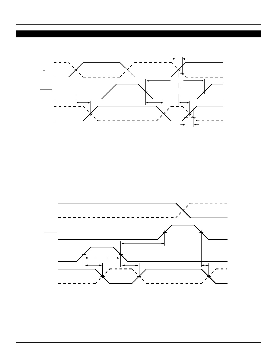
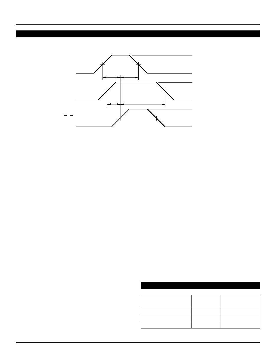
TIMING DIAGRAMS
Data Set-up and Hold Times
NOTES:
1. V
EE
= ≠4.2V to ≠5.5V unless otherwise specified; V
CC
= V
CCA
= GND
2. ts is the minimum time before the transition of the clock that information
must be present at the data input.
3. t
H
is the minimum time after the transition of the clock that information must
remain unchanged at the data input.
PRODUCT ORDERING CODE
Ordering
Package
Operating
Code
Type
Range
SY100S355FC
F24-1
Commercial
SY100S355JC
J28-1
Commercial
SY100S355JCTR
J28-1
Commercial
DATA
50%
≠1.69V
S
0
, S
1
t
S
t
H
≠0.95V
≠1.69
≠0.95V
50%
≠1.69V
E
1
, E
2
≠0.95V
50%
t
S
t
H