
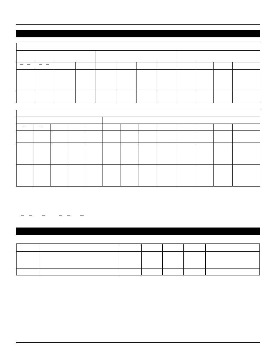
Pin
Function
A
na
, A
nb
Address Inputs (n = 0,1,2)
E
na
, E
nb
Enable Inputs (n = 1,2)
M
Mode Control Input
H
a
Z
0
≠ Z
3
(Z
0a
≠ Z
3a
) Polarity Select Input
H
b
Z
4
≠ Z
7
(Z
0b
≠ Z
3b
) Polarity Select Input
H
c
Common Polarity Select Input
Z
0
≠ Z
7
Single 1-of-8 Data Outputs
Z
na
, Z
nb
Dual 1-of-4 Data Outputs (n = 1...4)
V
EES
V
EE
Substrate
V
CCA
V
CCO
for ECL Outputs
SY100S370
UNIVERSAL
DEMULTIPLEXER/
DECODER
FEATURES
s
Max. propagation delay of 1200ps
s
I
EE
min. of ≠92mA
s
Industry standard 100K ECL levels
s
Extended supply voltage option:
V
EE
= ≠4.2V to ≠5.5V
s
Voltage and temperature compensation for improved
noise immunity
s
Internal 75K
input pull-down resistors
s
60% faster than National or Signetics
s
Approximately 40% lower power than Fairchild
s
Function and pinout compatible with Fairchild F100K
s
Available in 24-pin CERPACK and 28-pin PLCC
packages
DESCRIPTION
The SY100S370 is a universal demultiplexer/decoder
that can be used as either a dual 1-of-4 decoder or as a
single 1-of-8 decoder and is designed for use in high-
performance ECL systems. The Mode control (M) input
determines the function. In the dual 1-of-4 mode, each 4-
input group has a pair of active-LOW Enable (E) inputs.
The Enable pins are assigned such that in the single 1-of-
8 mode they can be tied together in pairs to result in two
active-LOW Enable inputs. E
1a
will be tied to E
1b
and E
2a
to E
2b
.
The auxiliary inputs (H
n
) are used to determine whether
the outputs are active-HIGH or active-LOW. The address
inputs for the dual 1-of-4 mode are A
0a
, A
1a
, A
0b
. A
2a
is
unused. In the 1-of-8 mode, the address inputs are A
0a
,
A
1a
, A
2a
. The inputs on the device have 75K
pull-down
resistors.
PIN NAMES
Rev.: G
Amendment: /0
Issue Date:
July, 1999
H
a
E
2
a
E
2
b
V
EE
E
1b
E
1a
A
2a
M
A
1a
A
0a
Z
2a
(Z
2
)
Z
1a
(Z
1
)
H
c
A
0b
Z
3b
(Z
7
)
H
b
Z
0b
(Z
4
)
A
1b
18
17
16
15
14
13
1
2
3
4
5
6
7
24
8
23
9
22
10
21
11
20
12
19
Top View
Flatpack
F24-1
V
CC
V
CCA
Z
1b
(Z
5
)
Z
3a
(Z
3
)
Z
2b
(Z
6
)
Z
0a
(Z
0
)
PIN CONFIGURATIONS
Z
0a
(Z
0
)
Z
3a
(Z
3
)
V
CCA
V
CC
Z
1b
(Z
5
)
V
CC
E
1a
V
EE
E
2b
E
1b
E
2a
V
EES
4
3
2
1
28
27
12
13
14
15
16
17
19
11
20
10
21
9
22
8
23
7
24
6
Top View
PLCC
J28-1
Z
2b
(Z
6
)
H
a
26
18
25
5
A
2a
M
A
1a
V
EES
A
0a
Z
1a
(Z
1
)
Z
2a
(Z
2
)
A
0b
V
EES
H
b
A
1b
H
c
Z
3b
(Z
7
)
Z
0b
(Z
4
)
1
3
SY100S370
Micrel
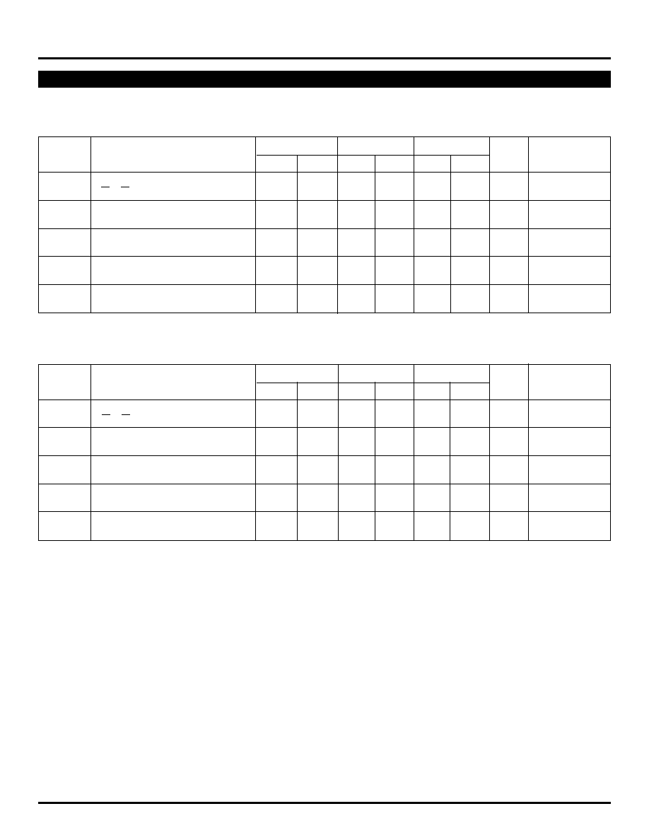
Single 1-of-8 Mode (M = HIGH; A
0b
= A
1b
= H
a
= H
b
= LOW)
Inputs
Active HIGH Outputs* (H
c
Input HIGH)
E
1
E
2
A
2a
A
1a
A
0a
Z
0
Z
1
Z
2
Z
3
Z
4
Z
5
Z
6
Z
7
H
X
X
X
X
L
L
L
L
L
L
L
L
X
H
X
X
X
L
L
L
L
L
L
L
L
L
L
L
L
L
H
L
L
L
L
L
L
L
L
L
L
L
H
L
H
L
L
L
L
L
L
L
L
L
H
L
L
L
H
L
L
L
L
L
L
L
L
H
H
L
L
L
H
L
L
L
L
L
L
H
L
L
L
L
L
L
H
L
L
L
L
L
H
L
H
L
L
L
L
L
H
L
L
L
L
H
H
L
L
L
L
L
L
L
H
L
L
L
H
H
H
L
L
L
L
L
L
L
H
TRUTH TABLES
(1)
Dual 1-of-4 Mode (M = A
2a
= H
c
= LOW)
Active HIGH Outputs
Active LOW Outputs
Inputs
(H
a
and H
b
Inputs HIGH)
(H
a
and H
b
Inputs LOW)
E
1a
,E
1b
E
2a
,E
2b
A
1a
,A
1b
A
0a
,A
0b
Z
0a
,Z
0b
Z
1a
,Z
1b
Z
2a
,Z
2b
Z
3a
,Z
3b
Z
0a
,Z
0b
Z
1a
,Z
1b
Z
2a
,Z
2b
Z
3a
,Z
3b
H
X
X
X
L
L
L
L
H
H
H
H
X
H
X
X
L
L
L
L
H
H
H
H
L
L
L
L
H
L
L
L
L
H
H
H
L
L
L
H
L
H
L
L
H
L
H
H
L
L
H
L
L
L
H
L
H
H
L
H
L
L
H
H
L
L
L
H
H
H
H
L
NOTE:
1. H = HIGH Voltage Level
L = LOW Voltage Level
X = Don't Care
* for H
c
= LOW, output states are complemented
E
1
= E
1a
and E
1b
wired; E
2
= E
2a
and E
2b
wired
DC ELECTRICAL CHARACTERISTICS
V
EE
= ≠4.2V to ≠5.5V unless otherwise specified; V
CC
= V
CCA
= GND
Symbol
Parameter
Min.
Typ.
Max.
Unit
Condition
I
IH
Input HIGH Current
µ
A
V
IN
= V
IH
(Max.)
Hc, A0a, A1a, A2a
--
--
310
All Others
--
--
250
I
EE
Power Supply Current
≠92
≠73
≠46
mA
Inputs Open
4
SY100S370
Micrel
AC ELECTRICAL CHARACTERISTICS
CERPACK
V
EE
= ≠4.2V to ≠5.5V unless otherwise specified; V
CC
= V
CCA
= GND
PLCC
V
EE
= ≠4.2V to ≠5.5V unless otherwise specified; V
CC
= V
CCA
= GND
T
A
= 0
∞
C
T
A
= +25
∞
C
T
A
= +85
∞
C
Symbol
Parameter
Min.
Max.
Min.
Max.
Min.
Max.
Unit
Condition
t
PLH
Propagation Delay
300
1300
300
1300
300
1300
ps
t
PHL
E
na
, E
nb
to Output
t
PLH
Propagation Delay
500
1600
500
1600
500
1600
ps
t
PHL
A
na
, A
nb
to Output
t
PLH
Propagation Delay
500
1600
500
1600
500
1600
ps
t
PHL
H
a
, H
b
, H
c
to Output
t
PLH
Propagation Delay
600
2100
600
2100
600
2100
ps
t
PHL
M to Output
t
TLH
Transition Time
300
900
300
900
300
900
ps
t
THL
20% to 80%, 80% to 20%
T
A
= 0
∞
C
T
A
= +25
∞
C
T
A
= +85
∞
C
Symbol
Parameter
Min.
Max.
Min.
Max.
Min.
Max.
Unit
Condition
t
PLH
Propagation Delay
300
1200
300
1200
300
1200
ps
t
PHL
E
na
, E
nb
to Output
t
PLH
Propagation Delay
500
1500
500
1500
500
1500
ps
t
PHL
A
na
, A
nb
to Output
t
PLH
Propagation Delay
500
1500
500
1500
500
1500
ps
t
PHL
H
a
, H
b
, H
c
to Output
t
PLH
Propagation Delay
600
2100
600
2100
600
2100
ps
t
PHL
M to Output
t
TLH
Transition Time
300
900
300
900
300
900
ps
t
THL
20% to 80%, 80% to 20%

