TRIPLE 4-INPUT
MULTIPLEXER
WITH ENABLE
SY100S371
FEATURES
s
Max. propagation delay of 1000ps
s
I
EE
min. of ≠68mA
s
Industry standard 100K ECL levels
s
Extended supply voltage option:
V
EE
= ≠4.2V to ≠5.5V
s
Voltage and temperature compensation for improved
noise immunity
s
Internal 75K
input pull-down resistors
s
40% faster than Fairchild
s
40% lower power than Fairchild
s
Function and pinout compatible with Fairchild F100K
s
Available in 24-pin CERPACK and 28-pin PLCC
packages
DESCRIPTION
The SY100S371 is an ultra-fast triple 4-input multiplexer
with true and complementary outputs designed for use in
high-performance ECL systems. The multiplexer is
controlled by common select inputs S
0
and S
1
. A logic
HIGH on the Enable (E) control input takes the outputs to
a logic LOW. The inputs on the device have 75K
pull-
down resistors.
Rev.: G
Amendment: /0
Issue Date:
July, 1999
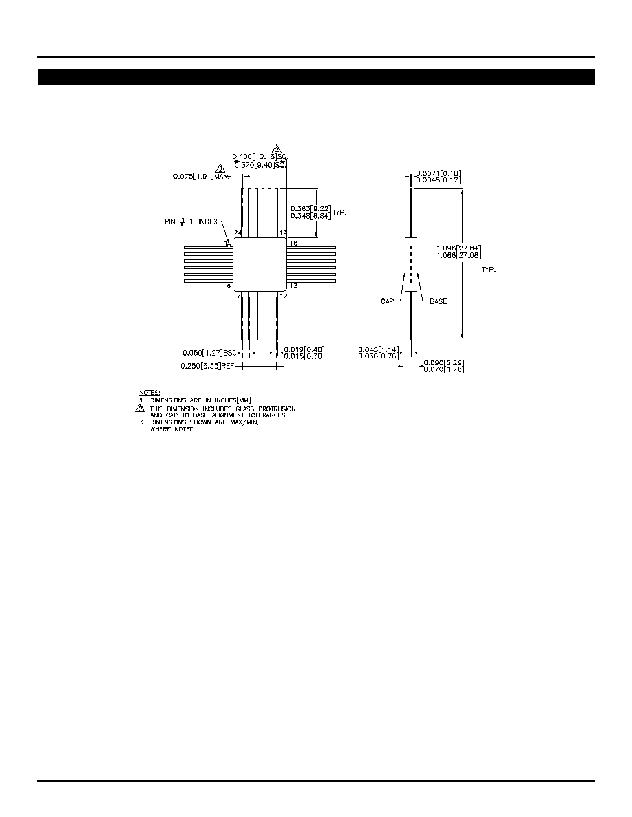
PIN CONFIGURATIONS
I
1b
I
0b
E
V
EE
S
1
S
0
I
3a
I
2a
I
1a
I
0a
Z
a
Z
a
I
2b
I
0c
I
2c
I
3b
I
3c
I
1c
18
17
16
15
14
13
1
2
3
4
5
6
7
24
8
23
9
22
10
21
11
20
12
19
Top View
Flatpack
F24-1
V
CC
V
CCA
Z
c
Z
b
Z
c
Z
b
Z
b
Z
b
V
CCA
V
CC
Z
c
V
CC
S
0
V
EE
E
S
1
I
0b
V
EES
4
3
2
1
28
27
12
13
14
15
16
17
19
11
20
10
21
9
22
8
23
7
24
6
Top View
PLCC
J28-1
Z
c
I
1b
26
18
25
5
I
3a
I
2a
I
1a
V
EES
I
0a
Z
a
Z
a
I
0c
V
EES
I
3b
I
1c
I
2b
I
2c
I
3c
BLOCK DIAGRAM
S
0
S
1
I
0a
I
1a
I
2a
I
3a
I
0b
I
1b
I
2b
I
3b
I
0c
I
1c
I
2c
I
3c
Z
a
Z
a
Z
b
Z
b
Z
c
Z
c
E
1
2
SY100S371
Micrel
Inputs
Outputs
E
S
0
S
1
Z
n
L
L
L
I
0X
L
H
L
I
1X
L
L
H
I
2X
L
H
H
I
3X
H
X
X
L
NOTE:
1. H = HIGH Voltage Level
L = LOW Voltage Level
X = Don't Care
TRUTH TABLE
(1)
DC ELECTRICAL CHARACTERISTICS
V
EE
= ≠4.2V to ≠5.5V unless otherwise specified; V
CC
= V
CCA
= GND
Symbol
Parameter
Min.
Typ.
Max.
Unit
Condition
I
IH
Input HIGH Current
µ
A
V
IN
= V
IH
(Max.)
I
0X
≠ I
3X
--
--
250
S
0
, S
1
, E
--
--
300
I
EE
Power Supply Current
≠68
≠48
≠34
mA
Inputs Open
Pin
Function
I
0X
≠ I
3X
Data Inputs (x = a, b or c)
S
0
, S
1
Select Inputs
E
Enable Input (Active LOW)
Z
a
≠ Z
c
Data Outputs
Z
a
≠ Z
c
Complementary Data Outputs
V
EES
V
EE
Substrate
V
CCA
V
CCO
for ECL Outputs
PIN NAMES
3
SY100S371
Micrel
T
A
= 0
∞
C
T
A
= +25
∞
C
T
A
= +85
∞
C
Symbol
Parameter
Min.
Max.
Min.
Max.
Min.
Max.
Unit
Condition
t
PLH
Propagation Delay
300
1100
300
1100
300
1100
ps
t
PHL
I
0X
≠ I
3X
to Output
t
PLH
Propagation Delay
400
1500
400
1500
400
1500
ps
t
PHL
S
0
, S
1
to Output
t
PLH
Propagation Delay
400
1400
400
1400
400
1400
ps
t
PHL
S
0
, S
1
to Output
t
TLH
Transition Time
300
900
300
900
300
900
ps
t
THL
20% to 80%, 80% to 20%
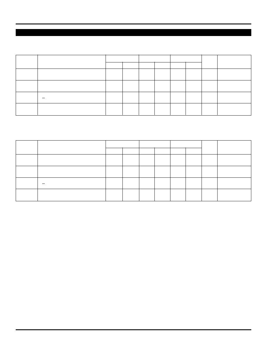
AC ELECTRICAL CHARACTERISTICS
CERPACK
V
EE
= ≠4.2V to ≠5.5V unless otherwise specified; V
CC
= V
CCA
= GND
PLCC
V
EE
= ≠4.2V to ≠5.5V unless otherwise specified; V
CC
= V
CCA
= GND
T
A
= 0
∞
C
T
A
= +25
∞
C
T
A
= +85
∞
C
Symbol
Parameter
Min.
Max.
Min.
Max.
Min.
Max.
Unit
Condition
t
PLH
Propagation Delay
300
1000
300
1000
300
1000
ps
t
PHL
I
0X
≠ I
3X
to Output
t
PLH
Propagation Delay
400
1400
400
1400
400
1400
ps
t
PHL
S
0
, S
1
to Output
t
PLH
Propagation Delay
400
1300
400
1300
400
1300
ps
t
PHL
S
0
, S
1
to Output
t
TLH
Transition Time
300
900
300
900
300
900
ps
t
THL
20% to 80%, 80% to 20%