FEATURES
DESCRIPTION
ClockWorksTM
SY100S811
Rev.: F
Amendment: /0
Issue Date: October, 1998
SINGLE SUPPLY 1:9
PECL/TTL-TO-PECL
s
PECL version of popular ECLinPS E111
s
Low skew
s
Guaranteed skew spec
s
V
BB
output
s
TTL enable input
s
Selectable TTL or PECL clock input
s
Single +5V supply
s
Differential internal design
s
Similar pin configuration to E111
s
PECL I/O fully compatible with industry standard
s
Internal 75K
PECL input pull-down resistors
s
Available in 28-pin PLCC and SOIC packages
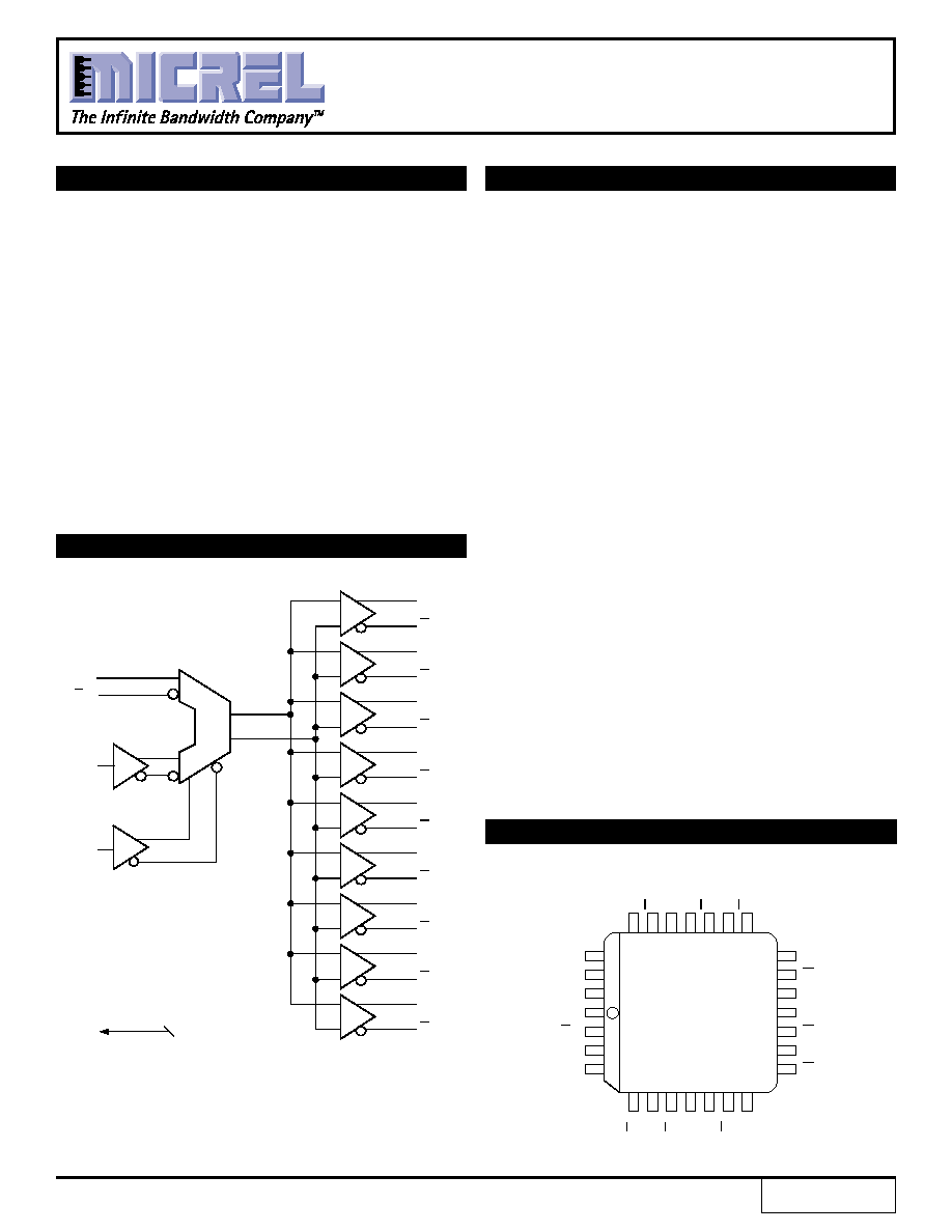
The SY100S811 is a low skew 1-to-9 PECL differential
driver designed for clock distribution in new, high-
performance PECL systems. It accepts either a PECL
clock input or a TTL input by using the TTL enable pin T
EN
.
When the TTL enable pin is HIGH, the TTL input is enabled
and the PECL input is disabled. When the enable pin is set
LOW, the TTL input is disabled and the PECL input is
enabled.
The device is specifically designed and produced for low
skew. The interconnect scheme and metal layout are
carefully optimized for minimal gate-to-gate skew within
the device. Wafer characterization and process control
ensure consistent distribution of propagation delay from lot
to lot. Since the S811 shares a common set of "basic"
processing with the other members of the ECLinPS family,
wafer characterization at the point of device personalization
allows for tighter control of parameters, including
propagation delay.
To ensure that the skew specification is met, it is
necessary that both sides of the differential output are
terminated into 50
, even if only one side is being used. ln
most applications, all nine differential pairs will be used
and, therefore, terminated. In the case where fewer than
nine pairs are used, it is necessary to terminate at least the
output pairs on the same package side (i.e. sharing the
same V
CCO
as the pair(s) being used on that side) in order
to maintain minimum skew.
The V
BB
output is intended for use as a reference
voltage for single-ended reception of PECL signals to that
device only. When using V
BB
for this purpose, it is
recommended that V
BB
is decoupled to V
CC
via a 0.01
µ
F
capacitor.
BLOCK DIAGRAM
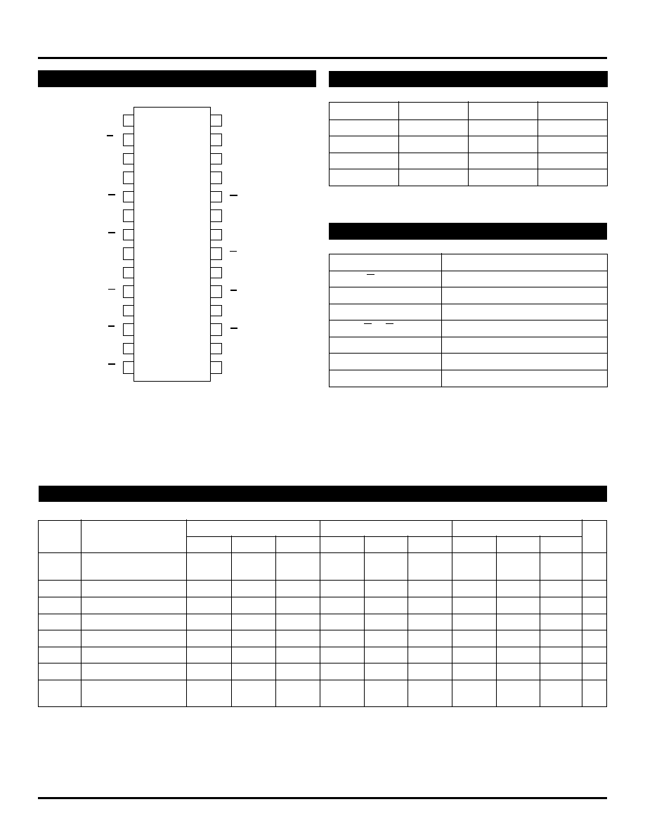
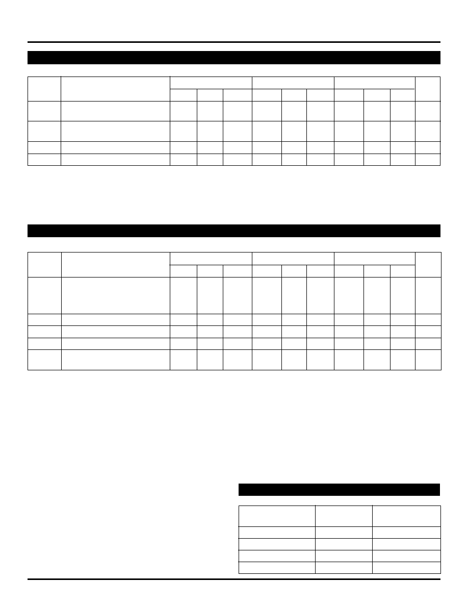
PIN CONFIGURATION
TOP VIEW
PLCC
J28-1
26
27
28
1
2
3
4
18
17
16
15
14
13
12
Q
3
Q
4
V
CCO
Q
5
Q
3
Q
4
Q
5
25 24 23 22 21 20 19
5
6
7
8
9
10 11
V
CC
V
EE
E
IN
V
BB
T
IN
T
EN
E
IN
V
CCO
Q
7
Q
6
Q
8
Q
8
Q
7
Q
6
Q
0
Q
1
V
CCO
Q
2
Q
0
Q
1
Q
2
V
BB
Q
0
Q
0
Q
1
Q
1
Q
2
Q
2
Q
3
Q
3
Q
4
Q
4
Q
5
Q
5
Q
6
Q
6
Q
7
Q
7
Q
8
Q
8
E
IN
E
IN
0
1
T
IN
T
EN
1
3
Micrel
TTL DC ELECTRICAL CHARACTERISTICS
AC ELECTRICAL CHARACTERISTICS
(1≠6)
NOTES:
1. Part-to-part skew is defined as Max. -- Min. value at the given temperature.
2. The differential propagation delay is defined as the delay from the crossing points of the differential input signals to the crossing point of the
differential output signals.
3. The single-ended propagation delay is defined as the delay from the 50% point of the input signal to the 50% point of the output signal.
4. The within-device skew is defined as the worst case difference between any two similar delay paths within a single device.
5. V
PP
(min.) is defined as the minimum input differential voltage which will cause no increase in the propagation delay. The V
PP
(min.) is AC limited for
the S811, as a differential input as low as 50mV will still produce full PECL levels at the output.
6. V
CMR
is defined as the range within which the V
IH
level may vary, with the device still meeting the propagation delay specification. The V
IL
level must
be such that the peak-to-peak voltage is less than 1.0V and greater than or equal to V
PP
(min.).
PRODUCT ORDERING CODE
Ordering
Package
Operating
Code
Type
Range
SY100S811JC
J28-1
Commercial
SY100S811JCTR
J28-1
Commercial
SY100S811ZC
Z28-1
Commercial
SY100S811ZCTR
Z28-1
Commercial
ClockWorksTM
SY100S811
V
CC
= V
CCO
= +5.0V
±
5%
T
A
= 0
∞
C
T
A
= +25
∞
C
T
A
= +85
∞
C
Symbol
Parameter
Min.
Typ.
Max.
Min.
Typ.
Max.
Min.
Typ.
Max.
Unit
V
IH
Input HIGH Voltage
2.0
--
--
2.0
--
--
2.0
--
--
V
V
IL
Input LOW Voltage
--
--
0.8
--
--
0.8
--
--
0.8
V
I
IH
Input HIGH Current
(1),(2)
--
--
20
--
--
20
--
--
20
µ
A
--
--
100
--
--
100
--
--
100
I
IL
Input LOW Current
(3)
--
--
≠0.6
--
--
≠0.6
--
--
≠0.6
mA
V
IK
Input Clamp Voltage
(4)
--
--
≠1.2
--
--
≠1.2
--
--
≠1.2
V
NOTES:
1.
V
IN
= 2.7V
2.
V
IN
= 5.0V
3.
V
IN
= 0.5V
4.
I
IN
= -18
mA
V
CC
= V
CCO
= +5.0V
±
5%
T
A
= 0
∞
C
T
A
= +25
∞
C
T
A
= +85
∞
C
Symbol
Parameter
Min.
Typ.
Max.
Min.
Typ.
Max.
Min.
Typ.
Max.
Unit
t
PLH
Propagation Delay to Output
(1)
ps
t
PHL
E
IN
(differential)
(2)
430
--
630
430
--
630
430
--
630
E
IN
(single-ended)
(3)
330
--
730
330
--
730
330
--
730
T
IN
350
--
950
350
--
950
350
--
950
t
skew
Within-Device skew
(4)
--
25
50
--
25
50
--
25
50
ps
V
PP
Minimum PECL Input Swing
(5)
250
--
--
250
--
--
250
--
--
mV
V
CMR
PECL Common Mode Range
(6)
≠1.6
--
≠0.4
≠1.6
--
≠0.4
≠1.6
--
≠0.4
V
t
r
Output Rise/Fall Times
275
375
600
275
375
600
275
375
600
ps
t
f
20% to 80%
5
Micrel
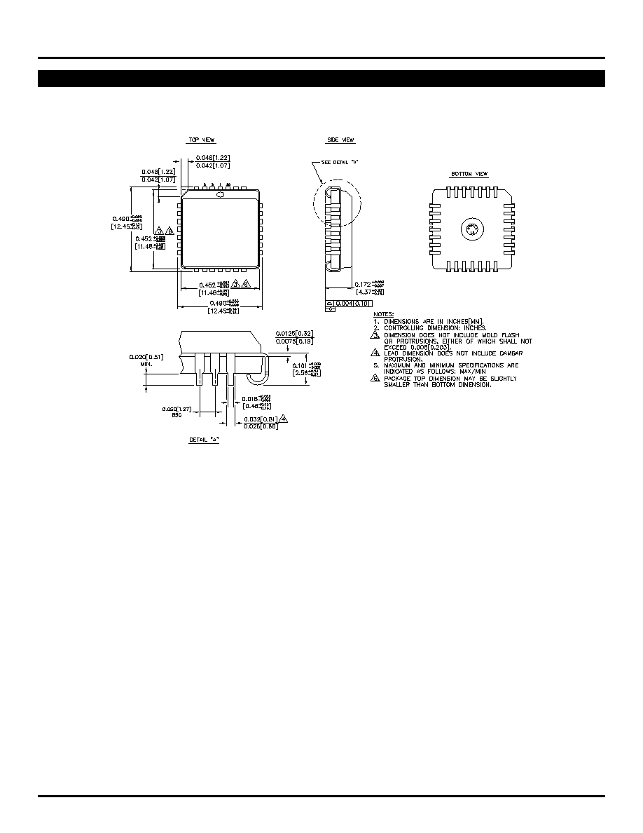
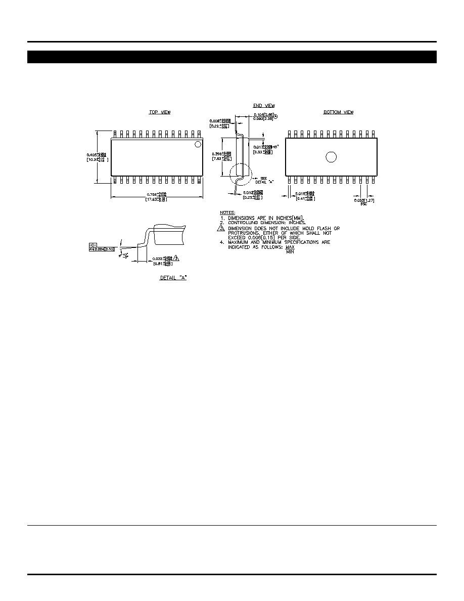
28 LEAD SOIC .300" WIDE (Z28-1)
Rev. 02
MICREL-SYNERGY
3250 SCOTT BOULEVARD
SANTA CLARA
CA 95054
USA
TEL
+ 1 (408) 980-9191
FAX
+ 1 (408) 914-7878
WEB
http://www.micrel.com
This information is believed to be accurate and reliable, however no responsibility is assumed by Micrel for its use nor for any infringement of patents or
other rights of third parties resulting from its use. No license is granted by implication or otherwise under any patent or patent right of Micrel Inc.
© 2000 Micrel Incorporated