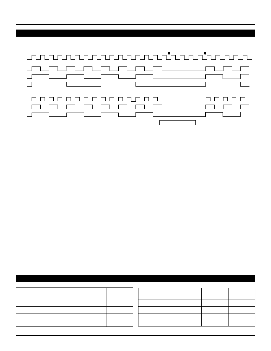
The SY100S834/L is low skew (
˜
1,
˜
2,
˜
4) or (
˜
2,
˜
4,
˜
8) clock generation chip designed explicitly for low
skew clock generation applications. The internal dividers
are synchronous to each other, therefore, the common
output edges are all precisely aligned. The devices can
be driven by either a differential or single-ended ECL or,
if positive power supplies are used, PECL input signal.
In addition, by using the V
BB
output, a sinusoidal source
can be AC-coupled into the device. If a single-ended
input is to be used, the V
BB
output should be connected
to the CLK input and bypassed to ground via a 0.01
µ
F
capacitor. The V
BB
output is designed to act as the
switching reference for the input of the SY100S834/L
under single-ended input conditions. As a result, this pin
can only source/sink up to 0.5mA of current.
The Function Select (F
SEL
) input is used to determine
what clock generation chip function is. When FS
EL
input
is LOW, SY100S834/L functions as a divide by 2, by 4
and by 8 clock generation chip. However, if FS
EL
input
is HIGH, it functions as a divide by 1, by 2 and by 4
clock generation chip. This latter feature will increase
the clock frequency by two folds.
The common enable (EN) is synchronous so that the
internal dividers will only be enabled/disabled when the
internal clock is already in the LOW state. This avoids
any chance of generating a runt clock pulse on the
internal clock when the device is enabled/disabled as
can happen with an asynchronous control. An internal
runt pulse could lead to losing synchronization between
the internal divider stages. The internal enable flip-flop is
clocked on the falling edge of the input clock, therefore,
all associated specification limits are referenced to the
negative edge of the clock input.
Upon start-up, the internal flip-flops will attain a random
state; the master reset (MR) input allows for the
synchronization of the internal dividers, as well as for
multiple SY100S834/Ls in a system.
DESCRIPTION
s
3.3V and 5V power supply options
s
50ps output-to-output skew
s
Synchronous enable/disable
s
Master Reset for synchronization
s
Internal 75K
input pull-down resistors
s
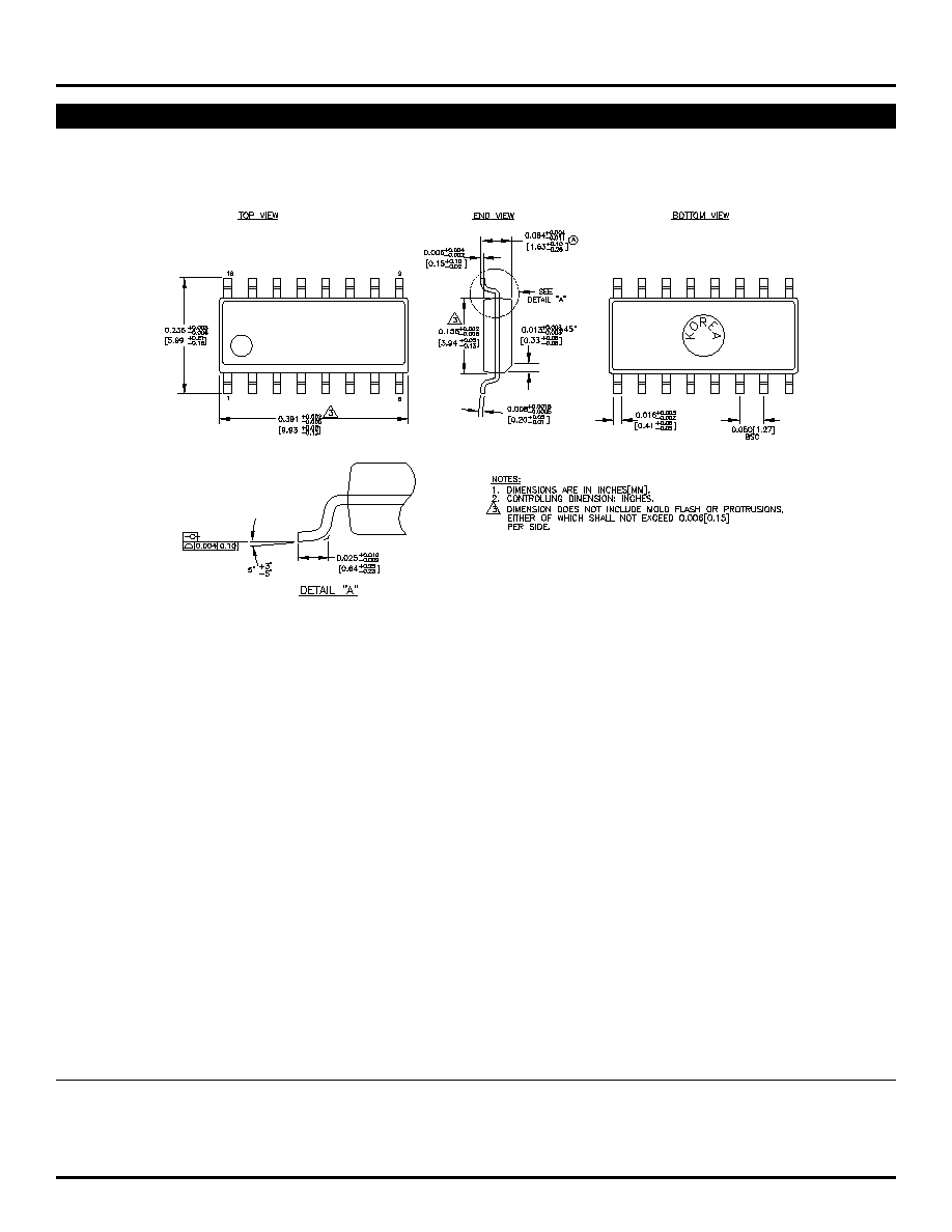
Available in 16-pin SOIC package
FEATURES
Rev.: F
Amendment: /0
Issue Date: September, 1999
(
˜
1,
˜
2,
˜
4) OR (
˜
2,
˜
4,
˜
8)
CLOCK GENERATION CHIP
ClockWorksTM
SY100S834
SY100S834L
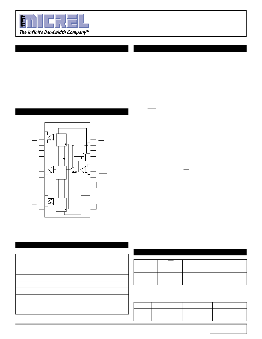
Pin
Function
CLK
Differential Clock Inputs
F
SEL
Function Select
EN
Synchronous Enable
MR
Master Reset
V
BB
Reference Output
Q
0
Differential
˜
1 or
˜
2 Outputs
Q
1
Differential
˜
2 or
˜
4 Outputs
Q
2
Differential
˜
4 or
˜
8 Outputs
PIN NAMES
CLK
EN
MR
Function
Z
L
L
Divide
ZZ
H
L
Hold Q
0≠2
X
X
H
Reset Q
0≠2
NOTES:
Z = LOW-to-HIGH transition
ZZ = HIGH-to-LOW transition
TRUTH TABLE
F
SEL
Q
0
Outputs
Q
1
Outputs
Q
2
Outputs
L
Divide by 2
Divide by 4
Divide by 8
H
Divide by 1
Divide by 2
Divide by 4
PIN CONFIGURATION/BLOCK DIAGRAM
SOIC
TOP VIEW
V
CC
EN
F
SEL
CLK
CLK
V
BB
MR
V
EE
Q
0
Q
0
V
CC
Q
1
Q
1
V
CC
Q
2
Q
2
16
15
14
13
12
11
10
9
1
2
3
4
5
6
7
8
Q
R
Q
R
˜
1 or
˜
2
Q
Q
R
R
D
˜
2 or
˜
4
˜
4 or
˜
8
1
2
ClockWorksTM
SY100S834
SY100S834L
Micrel
T
A
= ≠40
∞
C
T
A
= 0
∞
C
T
A
= +25
∞
C
T
A
= +85
∞
C
Symbol
Parameter
Min.
Typ.
Max.
Min.
Typ.
Max.
Min.
Typ.
Max.
Min.
Typ.
Max.
Unit
t
PLH
Propagation Delay
CLK
960
1100
1200
960
1100
1200
960
1100
1200
960
1100
1200
ps
t
PHL
to Output
MR
650
800
1010
650
800
1010
650
800
1010
650
800
1010
t
skew
Within-Device Skew
(2)
--
--
50
--
--
50
--
--
50
--
--
50
ps
t
S
Set-up Time EN
400
--
--
400
--
--
400
--
--
400
--
--
ps
t
H
Hold Time EN
200
--
--
200
--
--
200
--
--
200
--
--
ps
V
PP
Minimum Input Swing
250
--
--
250
--
--
250
--
--
250
--
--
mV
V
CMR
Common Mode Range
(3)
CLK
≠1.3
--
≠0.4
≠1.4
--
≠0.4
≠1.4
--
≠0.4
≠1.4
--
≠0.4
V
t
r
Output Rise/Fall Times
275
400
525
275
400
525
275
400
525
275
400
525
ps
t
f
Q (20% ≠ 80%)
AC ELECTRICAL CHARACTERISTICS
(1)
V
EE
= V
EE
(Min.) to V
EE
(Max.); V
CC
= GND
NOTES:
1. Parametric values specified at:
5 volt Power Supply Range
100S834 Series:
-4.2V to -5.5V.
3 volt Power Supply Range
100S834L Series
-3.0V to -3.8V.
2. Within-Device Skew is specified for identical transition.
3. The CMR range is referenced to the most positive side of the differential input signal. Normal operation is obtained if the HIGH level falls within the specified
range and the peak-to-peak voltage lies between V
PP
min. and 1V. The lower end of the CMR range varies 1:1 with V
EE
. The numbers in the spec table
assume a nominal V
EE
= ≠3.3V. Note for PECL operation, the V
CMR
(min) will be fixed at 3.3V ≠ IV
CMR
(min)I.
T
A
= ≠40
∞
C
T
A
= 0
∞
C
T
A
= +25
∞
C
T
A
= +85
∞
C
Symbol
Parameter
Min.
Typ.
Max.
Min.
Typ.
Max.
Min.
Typ.
Max.
Min.
Typ.
Max.
Unit
I
EE
Power Supply Current
--
--
49
--
--
49
--
--
49
--
--
54
mA
V
BB
Output Reference Voltage -1.38
--
-1.26
-1.38
--
-1.26
-1.38
--
-1.26
-1.38
--
-1.26
V
I
IH
Input HIGH Current
--
--
150
--
--
150
--
--
150
--
--
150
µ
A
DC ELECTRICAL CHARACTERISTICS
(1)
V
EE
= V
EE
(Min.) to V
EE
(Max.); V
CC
= GND
NOTE:
1. Parametric values specified at:
5 volt Power Supply Range
100S834 Series:
-4.2V to -5.5V.
3 volt Power Supply Range
100S834L Series
-3.0V to -3.8V.